


Printed Circuit Board Manufacturing丨Inner Layer Image Process
Multilayer PCB begins its inner core production with a chemical pre-clean which removes any residual matter and oxidation. Panels are fed directly into the clean room environment where a dry or wet film resist is applied and queued for exposure. This streamlined process minimizes costly handling and related defects.
The process of inner layer image exposure is to transfer inner layer images from artwork to the physical inner cores, it's carried out in cleanroom under controlled conditions. This ensures the best environment for artwork stability and cleanliness meaning we can image the most complex designs.
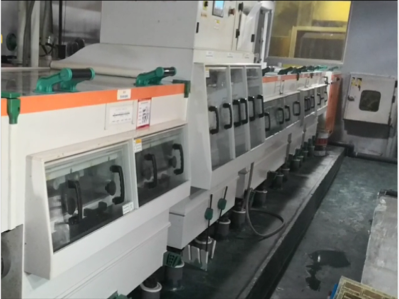
After exposure of artwork, multilayer PCB inner cores feed from clean rooms into an integrated system that develops, etches, and strips the inner layers. Inner layer process is to form inner layer circuitry of PCBs. This IS system is stainless steel and titanium. Computers control the parameters of the process, yielding consistent quality. Exiting the line is a finished core.
A-TECH use the most advanced Vacuum DES line in the industry, this is able to achieve the limit capability with minimum trace width/spacing 2/2mil, it's extremely suitable to build multilayer PCBs with fine traces and high density.
-
 Printed Circuit Board Manufacturing丨Inner Layer Image Process
 -
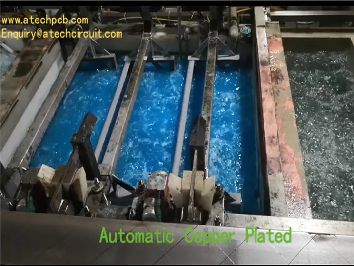 Automatic copper plated(PTH) - PCB fabrication process
 -
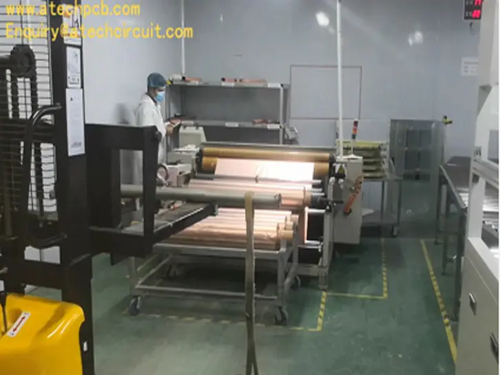
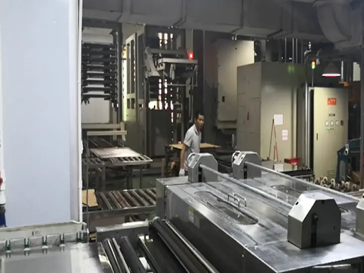 Lamination process of multilayer PCB
 -
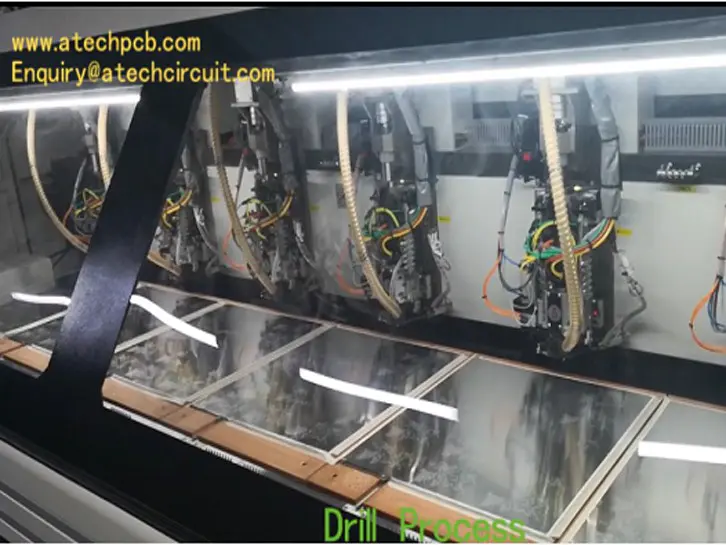 Drill process - China PCB manufacturing
 -
 Inner layer lay up before lamination - multilayer PCB fabrication
 -
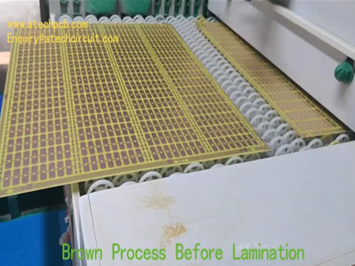 Brown process for multilayer PCB manufacturing
 -
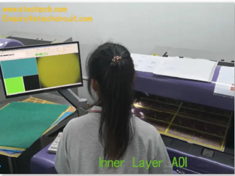 AOI for inner layer image - multilayer PCB manufacturing
 -
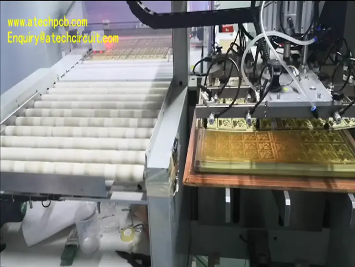 Online AOI For Multi-layer PCB Inner Layer After Etching


