Inner layer lay up before lamination - multilayer PCB fabrication
Before lamination process, the cores, PPs and copper foils need to be lay up with sequence according to stackup, and the layer to layer registration need to be controlled specially, this is one of key point for multilayer PCB manufacturing.
The copper foil used in circuit boards is typically in sheets of ½ oz. and 1 oz. per square foot in weight or 0.0007 and 0.00134 inches nominal thickness. In other words, one ounce of copper will cover one square foot when it is rolled out to a thickness of 0.00134" or 1.34 mils.
PP is the "glue" that holds the cores together. There are many types of materials, we use FR4–a woven fiberglass cloth pre- impregnated with epoxy resin - known in the industry as B-stage. The resin is activated and "melts" during the lamination process from pressure and heat. It flows across copper features and exposed laminate on the core and as it cools bonds the layers of foil and core together.
-
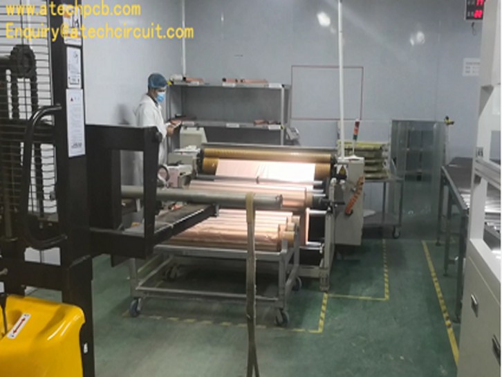 Inner layer lay up before lamination - multilayer PCB fabrication
 -
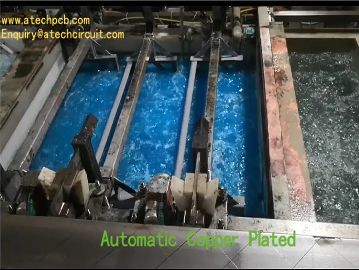 Automatic copper plated(PTH) - PCB fabrication process
 -
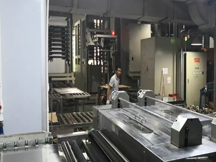 Lamination process of multilayer PCB
 -
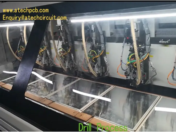 Drill process - China PCB manufacturing
 -
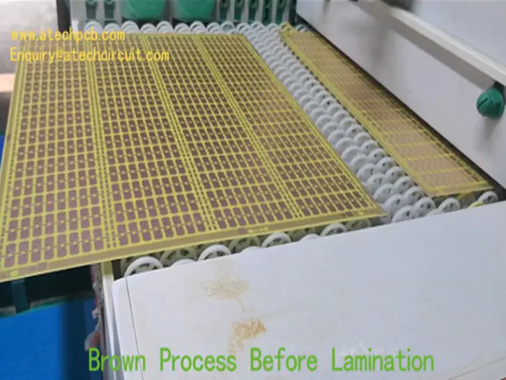 Brown process for multilayer PCB manufacturing
 -
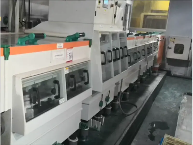 Printed Circuit Board Manufacturing丨Inner Layer Image Process
 -
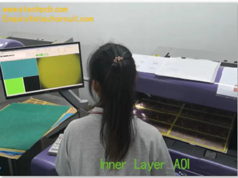 AOI for inner layer image - multilayer PCB manufacturing
 -
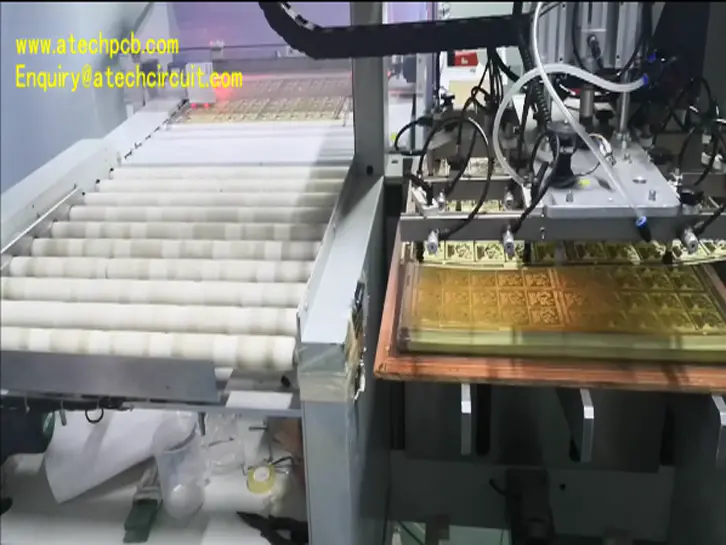 Online AOI For Multi-layer PCB Inner Layer After Etching


