


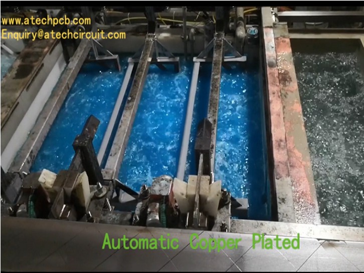
Automatic copper plated(PTH) - PCB fabrication process
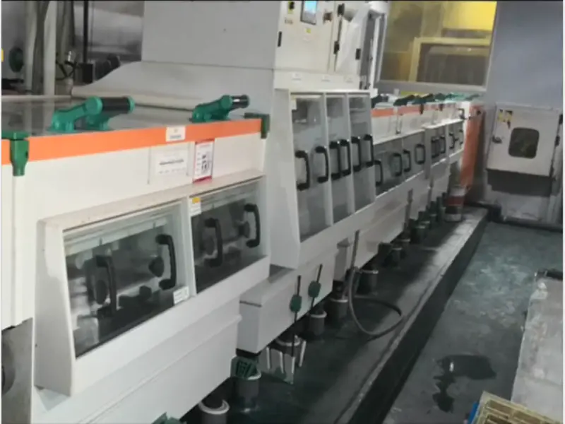
In order for the through holes to electrically connect to different layers of the PCB, a thin layer of copper is chemically deposited into the through holes and on the surface of copper, this copper will later be thickened through pattern plating process.
A-TECH add a desmear section in PTH line to reduce the roughness of through hole and guarantee high quality of plated copper in the holes.
Once the smear is removed, a thin coating of copper is chemically deposited on all of the exposed surfaces of the panel, including the hole walls. This creates a metallic base for electroplating copper into the holes and onto the surface. The thickness of the electroless deposit is between 45 & 60 millionths of an inch.
-
 Automatic copper plated(PTH) - PCB fabrication process
 -
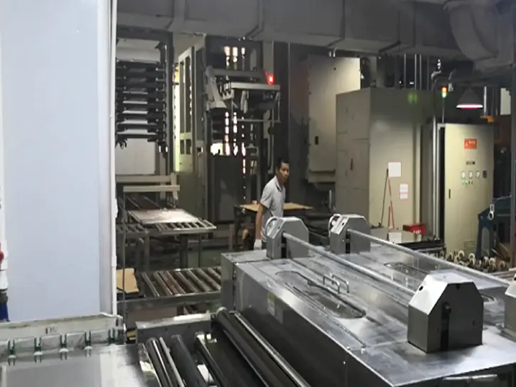 Lamination process of multilayer PCB
 -
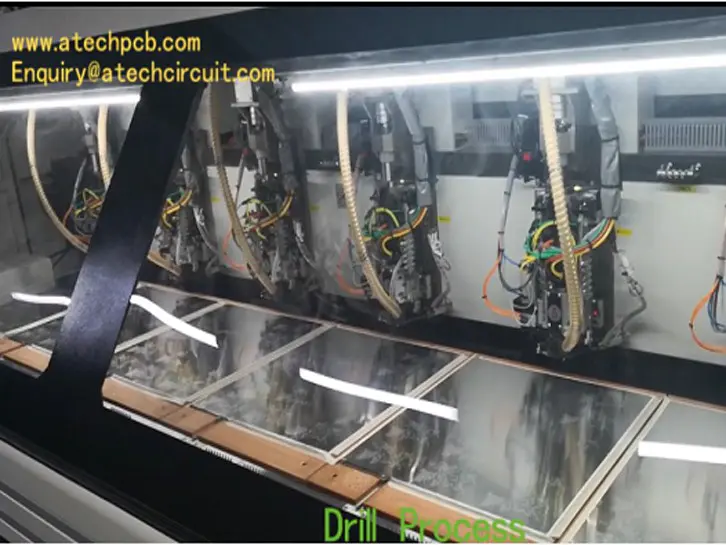 Drill process - China PCB manufacturing
 -
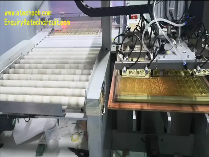
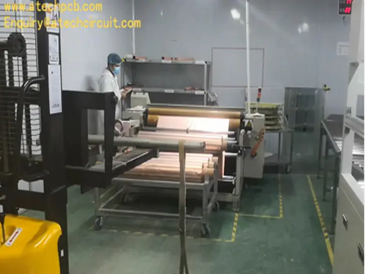 Inner layer lay up before lamination - multilayer PCB fabrication
 -
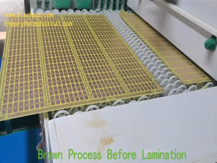 Brown process for multilayer PCB manufacturing
 -
 Printed Circuit Board Manufacturing丨Inner Layer Image Process
 -
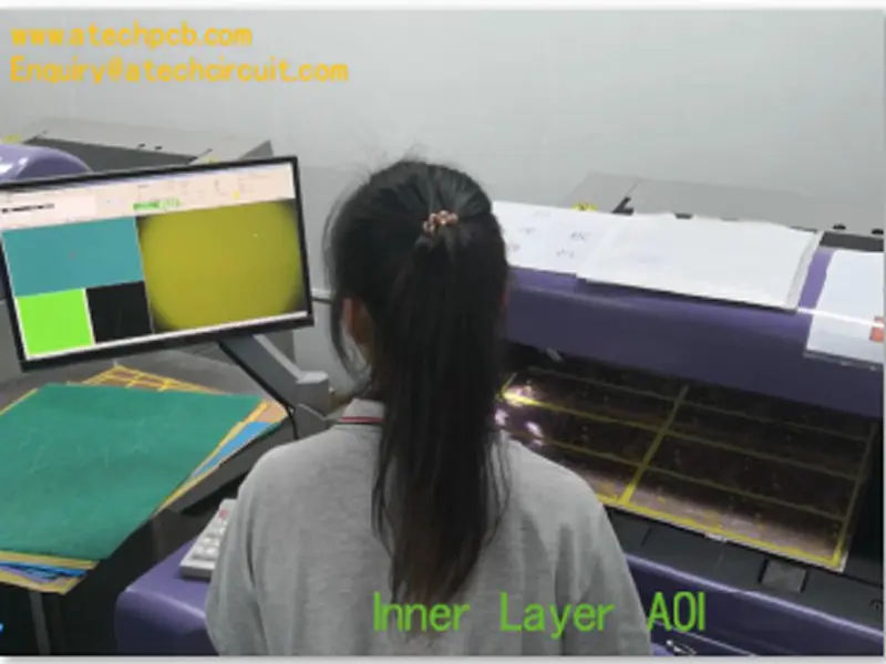 AOI for inner layer image - multilayer PCB manufacturing
 -
 Online AOI For Multi-layer PCB Inner Layer After Etching


