


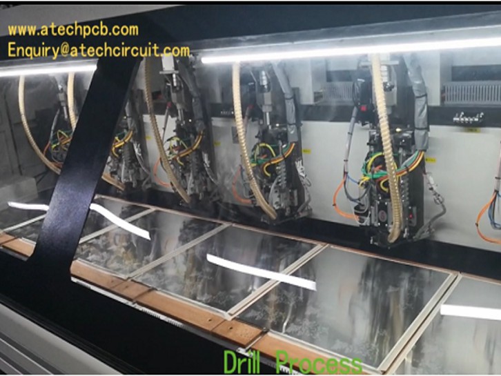
Drill process - China PCB manufacturing
Drilling is very critical to the PCB manufacturing process, holes of various sizes are drilled through a stack of working panels and the drilling process is computer numerical control.
Holes of various sizes are drilled through a stack of panels (usually 3 to 4 high). The locations are determined by the board’s designer to fit specific components. Drilled hole sizes are usually 8 mils larger than finished plated through hole sizes to allow for the copper plating process.
-
 Drill process - China PCB manufacturing
 -
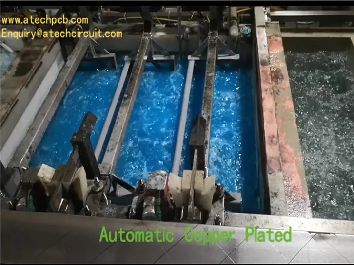 Automatic copper plated(PTH) - PCB fabrication process
 -
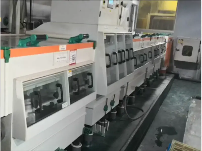
 Lamination process of multilayer PCB
 -
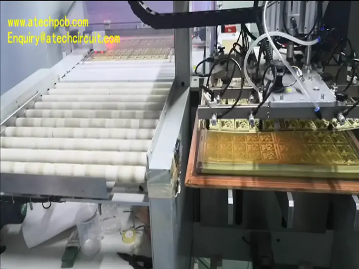
 Inner layer lay up before lamination - multilayer PCB fabrication
 -
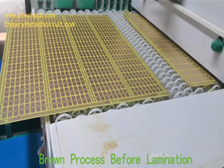 Brown process for multilayer PCB manufacturing
 -
 Printed Circuit Board Manufacturing丨Inner Layer Image Process
 -
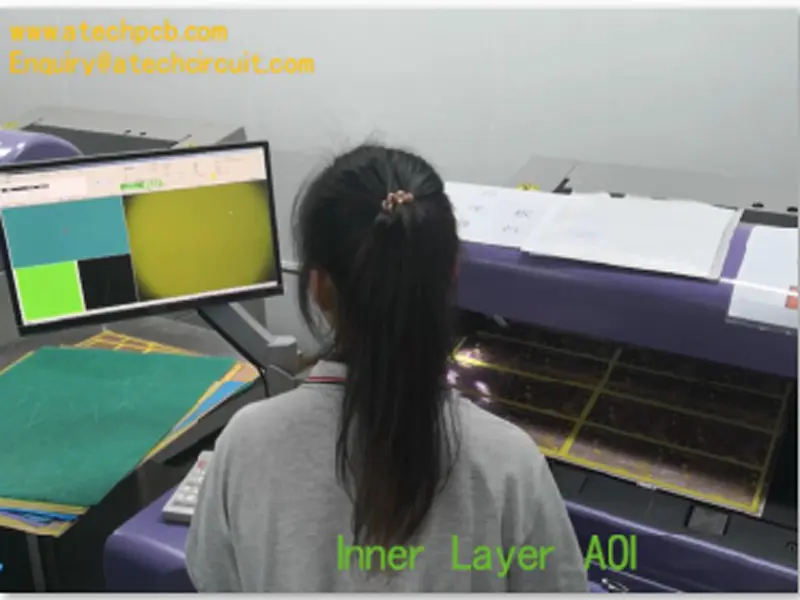 AOI for inner layer image - multilayer PCB manufacturing
 -
 Online AOI For Multi-layer PCB Inner Layer After Etching


