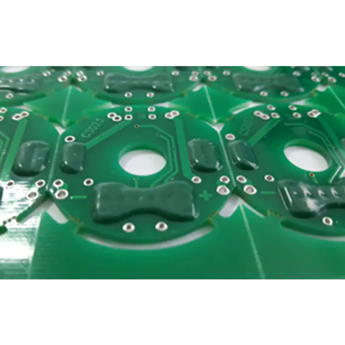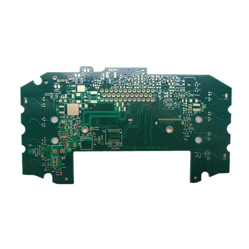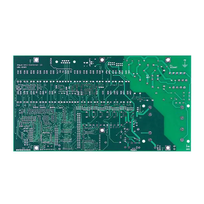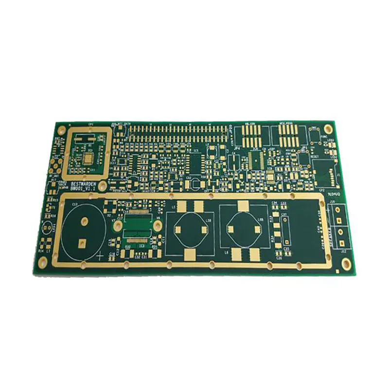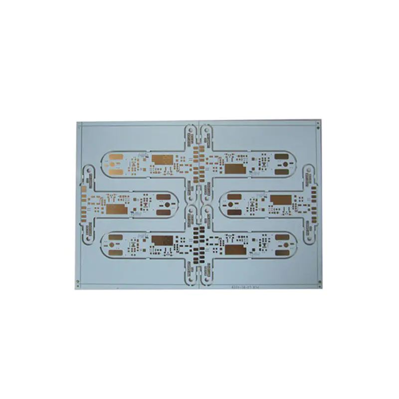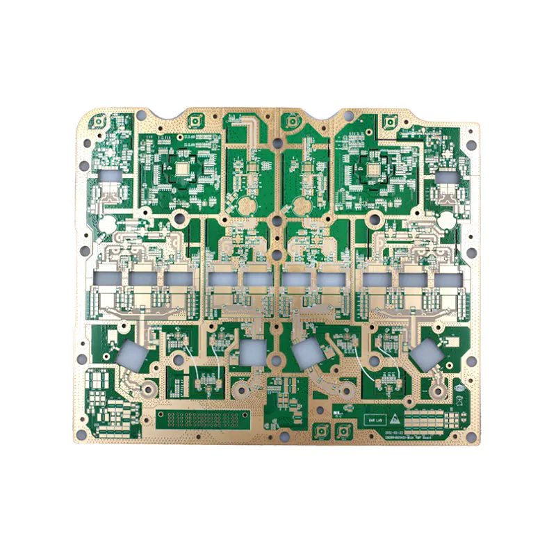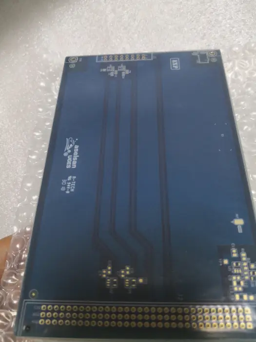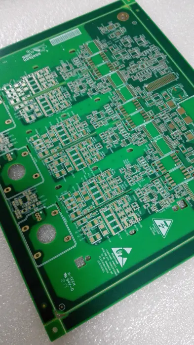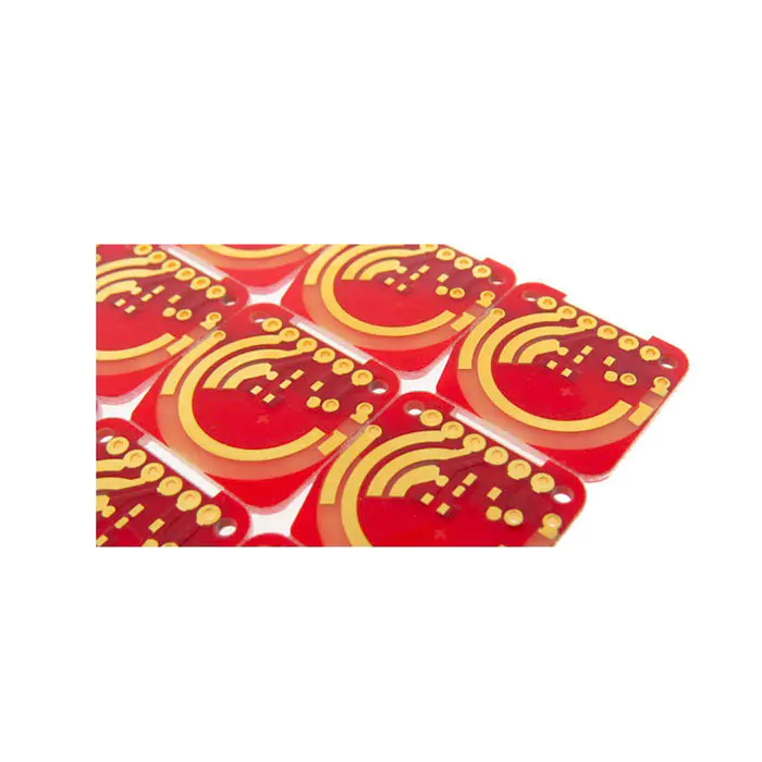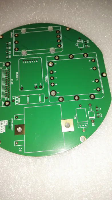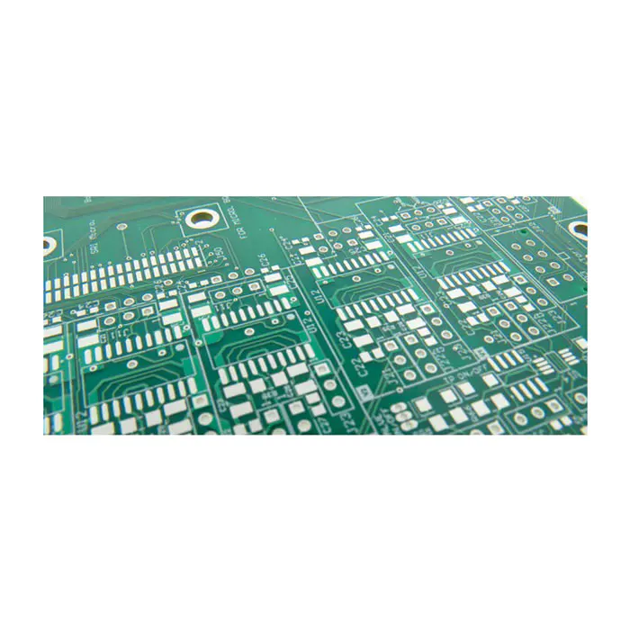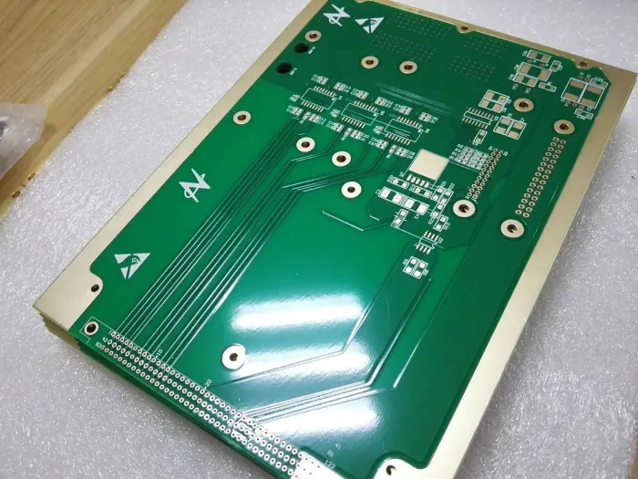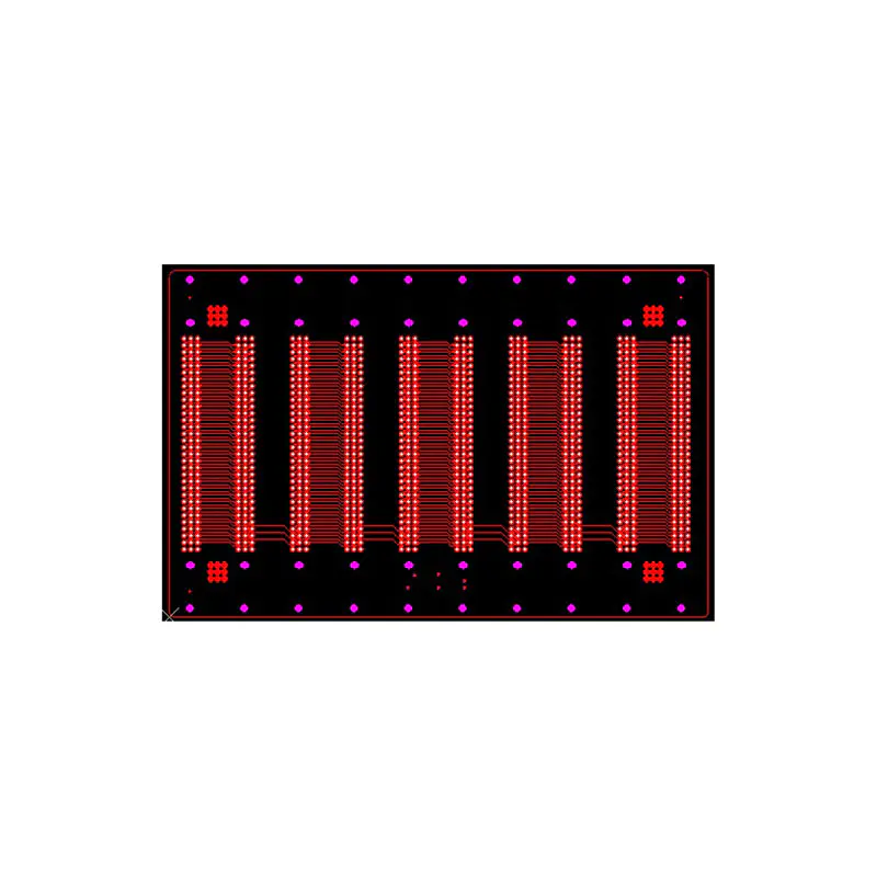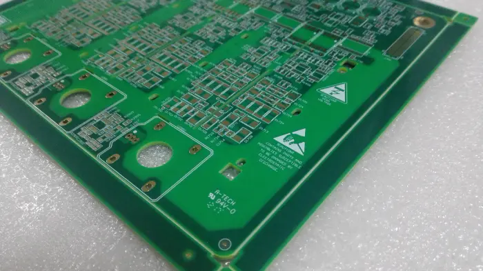
Double-sided PCB
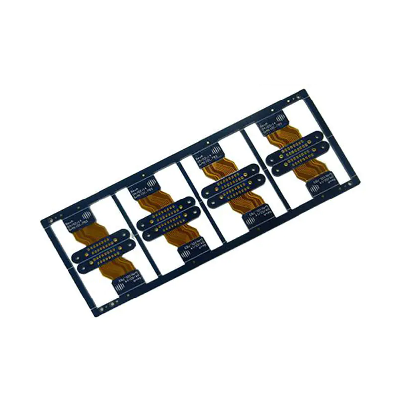
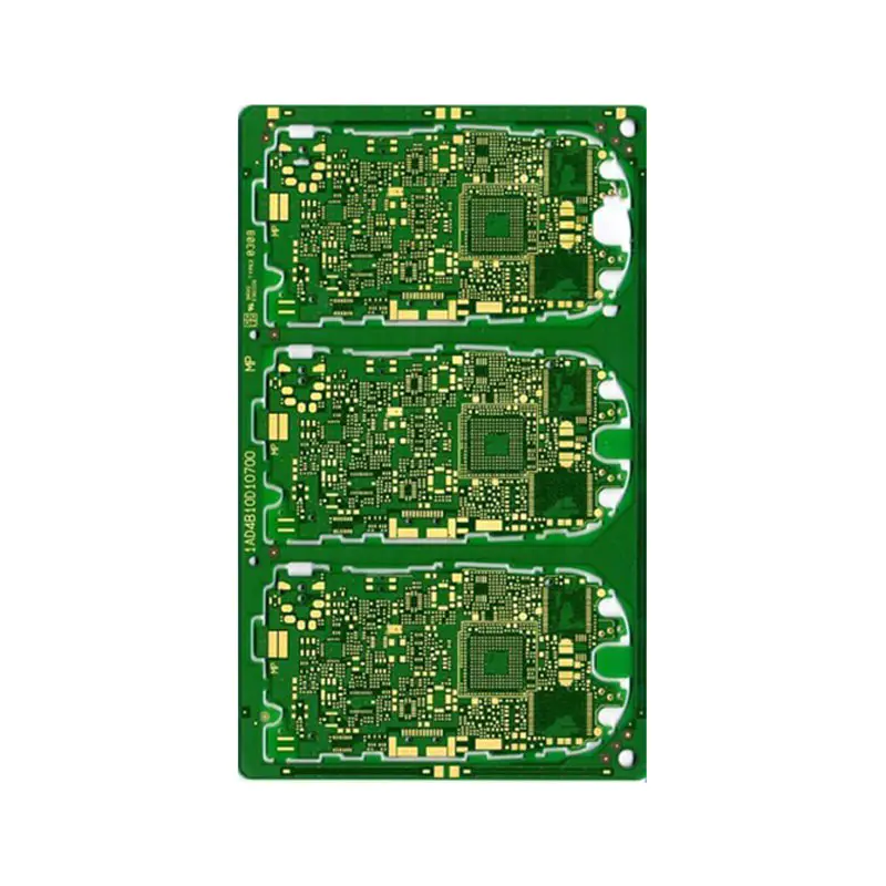
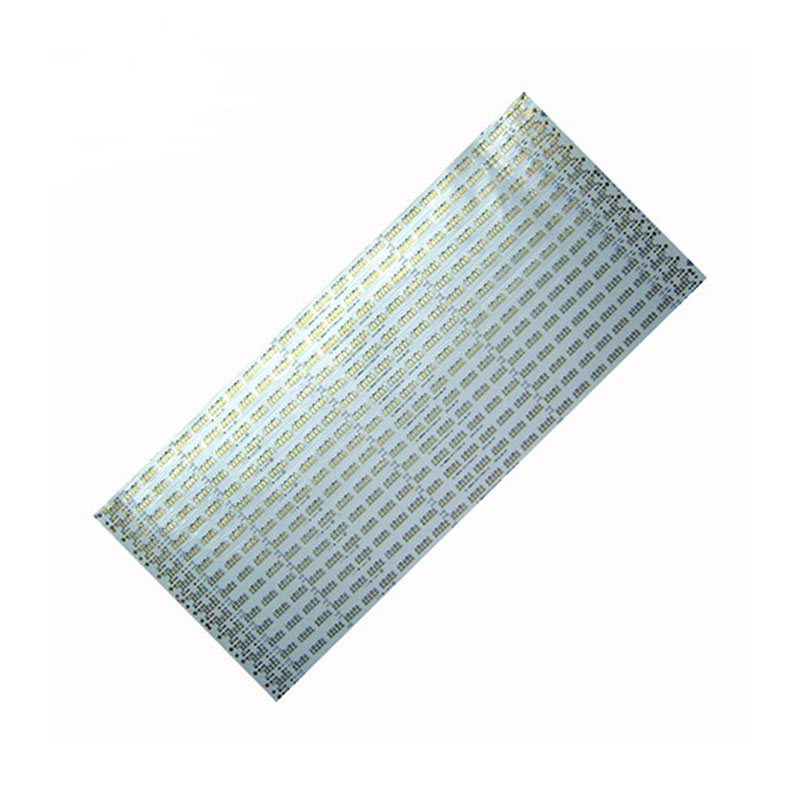
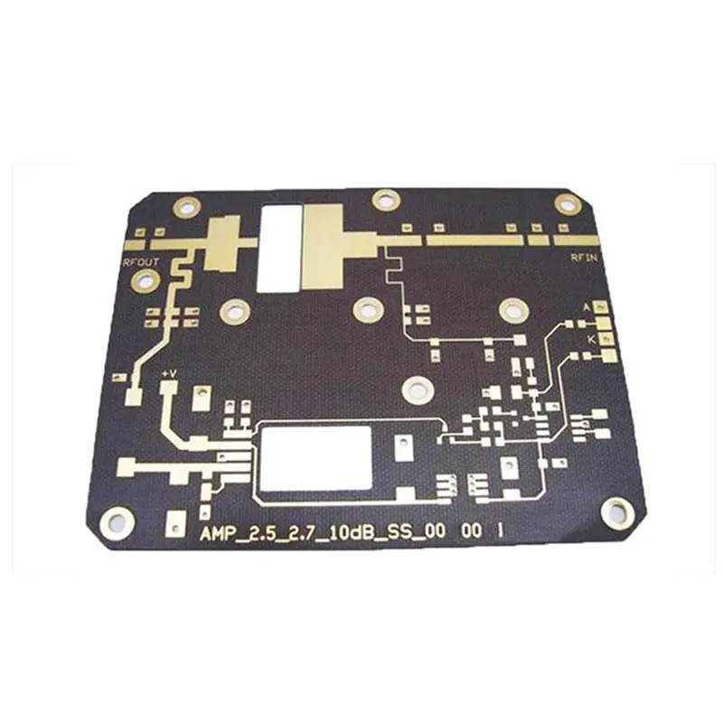
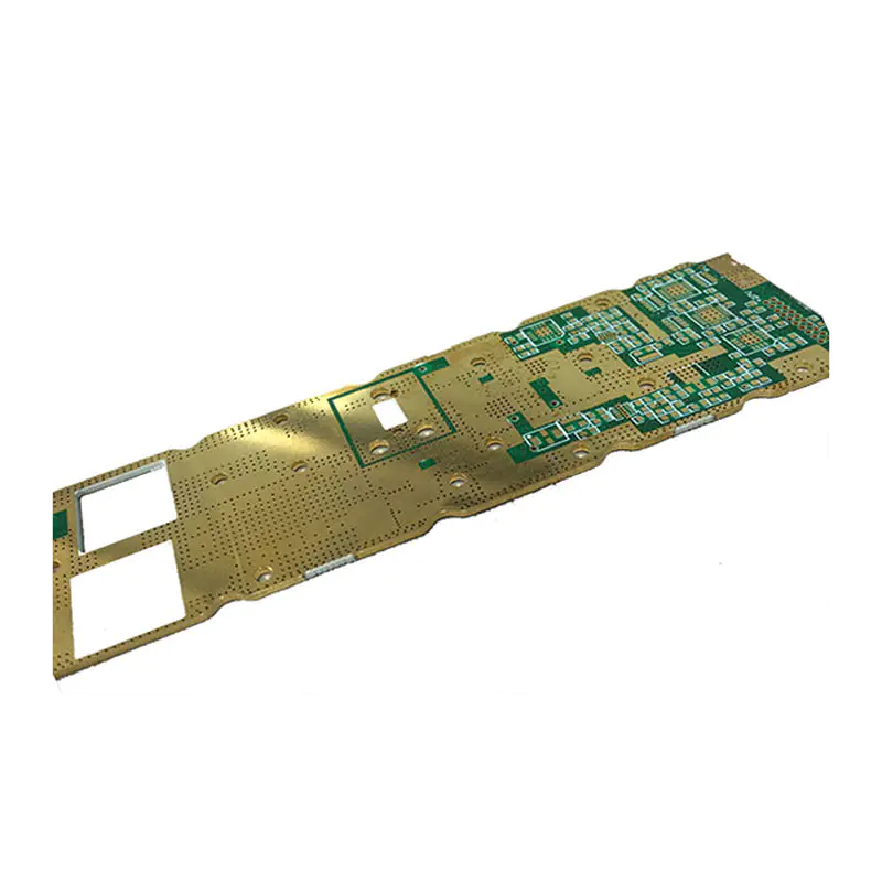
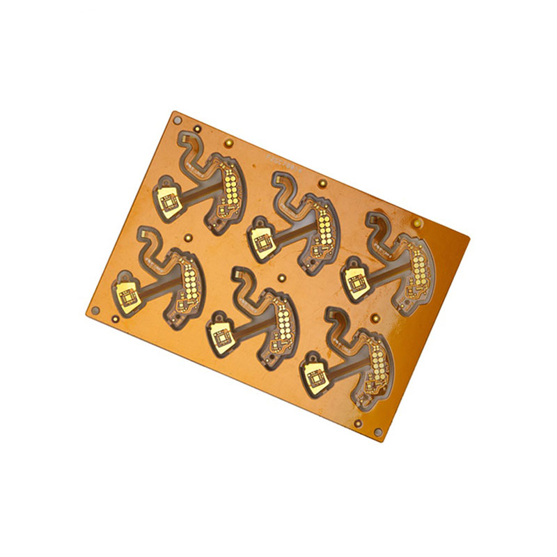
Related Products


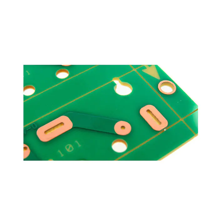
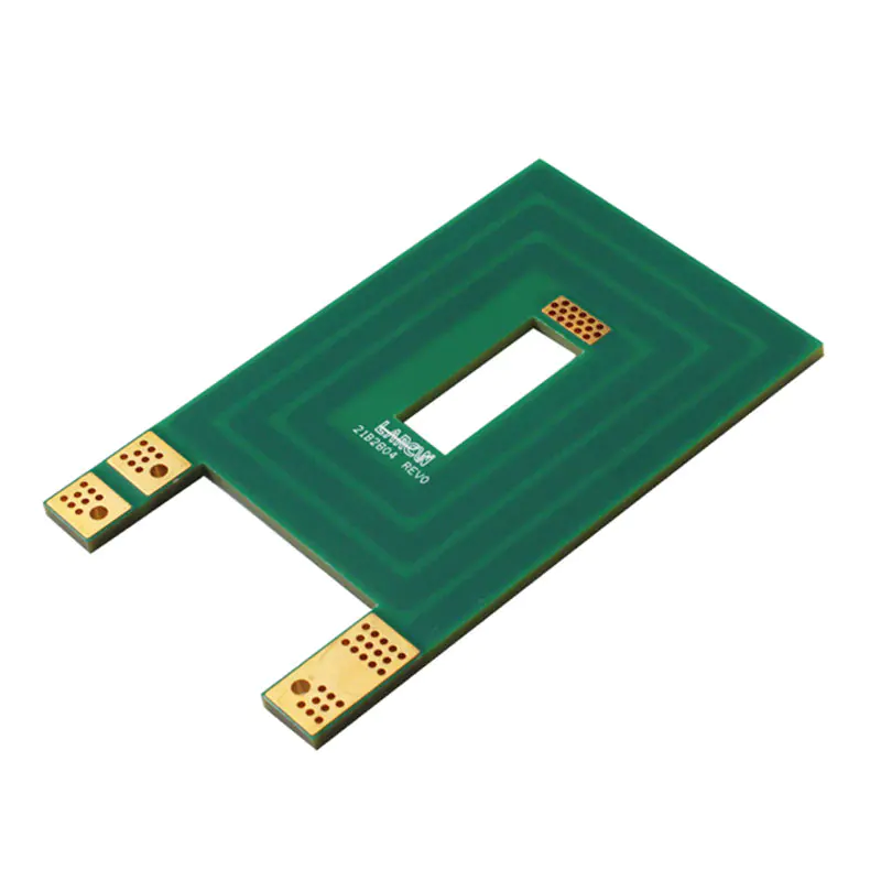
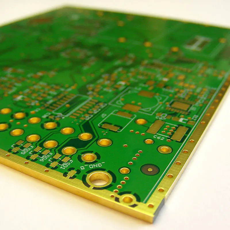
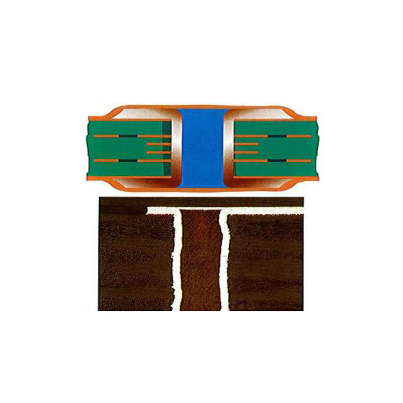
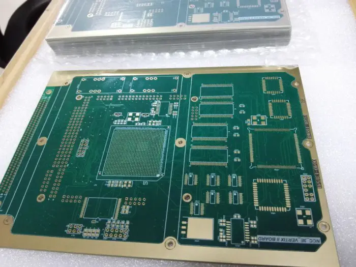
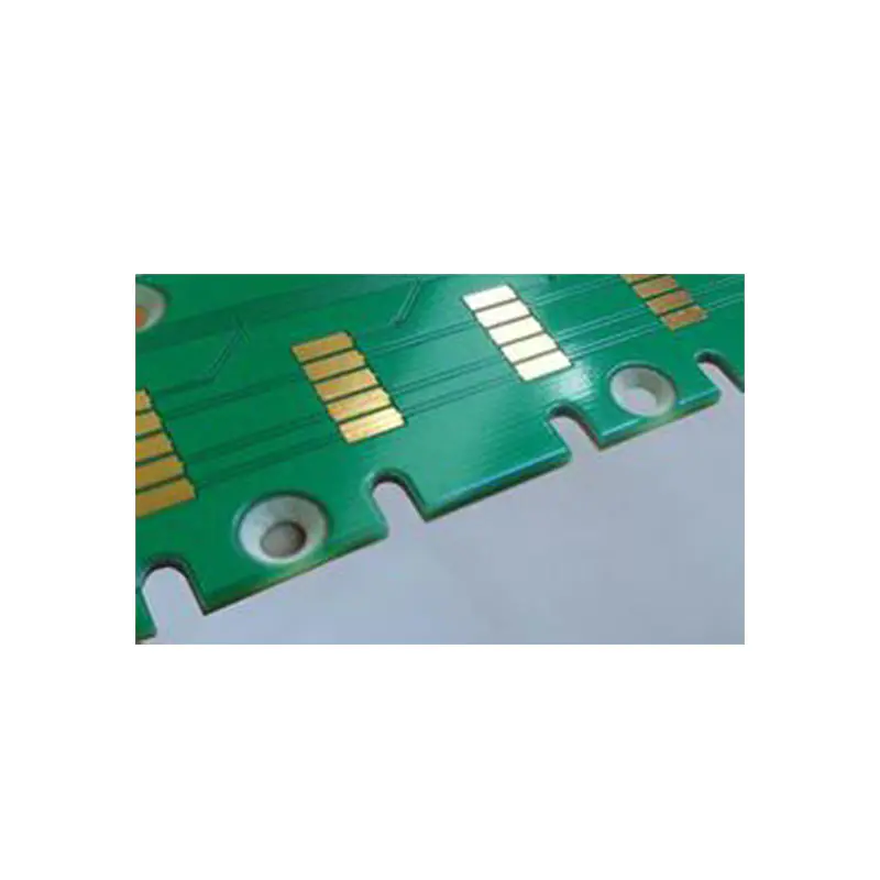
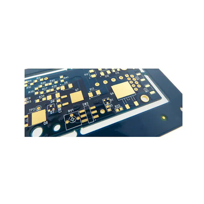
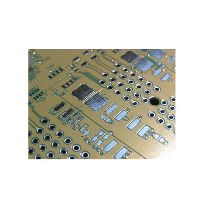
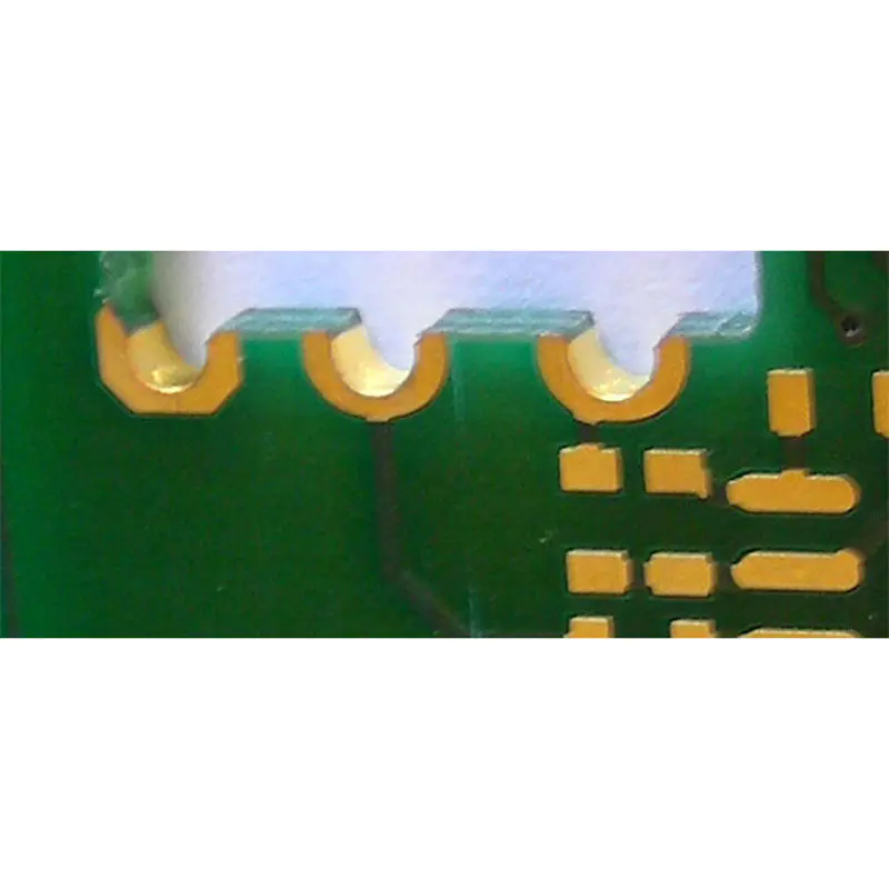
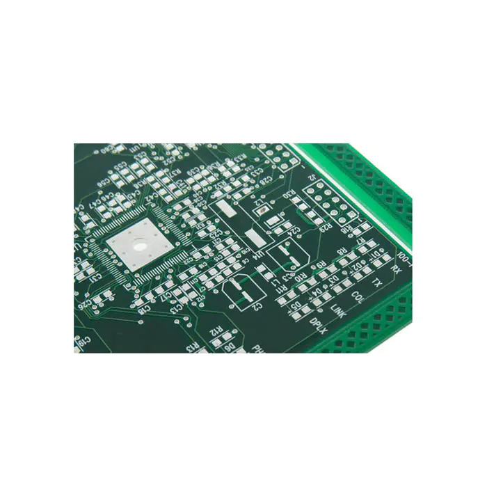
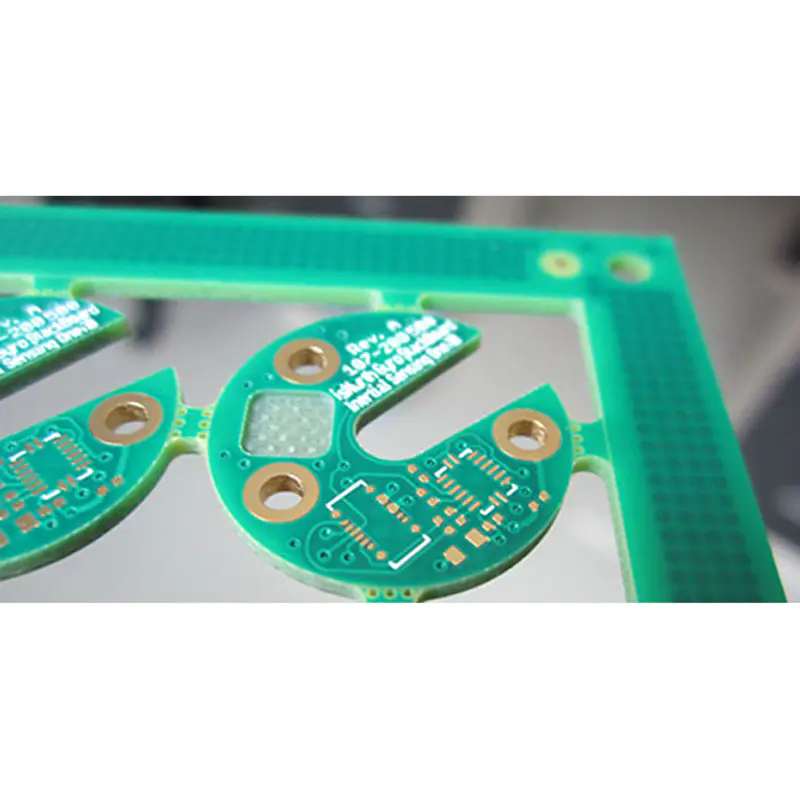
PCB edge plating, also called sideplating, it refers to copper plating that runs from top side to bottom side and runs along at least one of the perimeter edges. Portions of the printed circuit’s contour but also partial areas within the circuit board can be metalized.
In order to make PCB edges metalized, the printed circuit boards must be routed before through hole copper plated process, because the metallization of the PCB edges take place during this copper plating process. The ENIG (Immersion Gold) finish is preferred for PCB edges after copper plated.
PCB edge plating technology is used for several industries, especially in application that require better support function, such as:
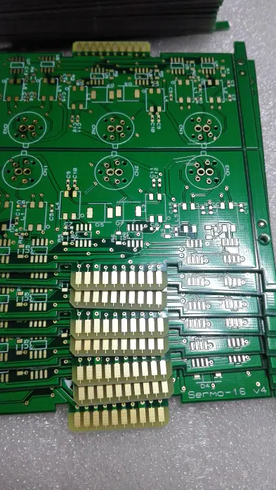
● Edge connections and protection
● Edge soldering to improve fabrication
● Better support for connections such as boards that slide into housing connection
● Improving current-carrying capabilities for better EMC performance such as high frequency PCB
A-TECH has lots of manufacturing experience for PCB edge plating, and we’re able to control high quality for edge plating without burrs. Please try to contact our sales experts for any technical details.
General inquiries & Customer Service
Tel: 86-755-2335 9039 | Fax: 86-755-3318 0939
E-Mail: Enquiry@atechcircuit.com
Skype: atechcircuits

Headquarters: 602, Building B3, Zhimei Huizhi Industrial Park, Fuyong Street, Bao'an District, Shenzhen City, China
Copyright © 2025 A-TECH CIRCUITS Co., Ltd. | All Rights Reserved
Hello, please leave your name and email here before chat online so that we won't miss your message and contact you smoothly.