Related Products

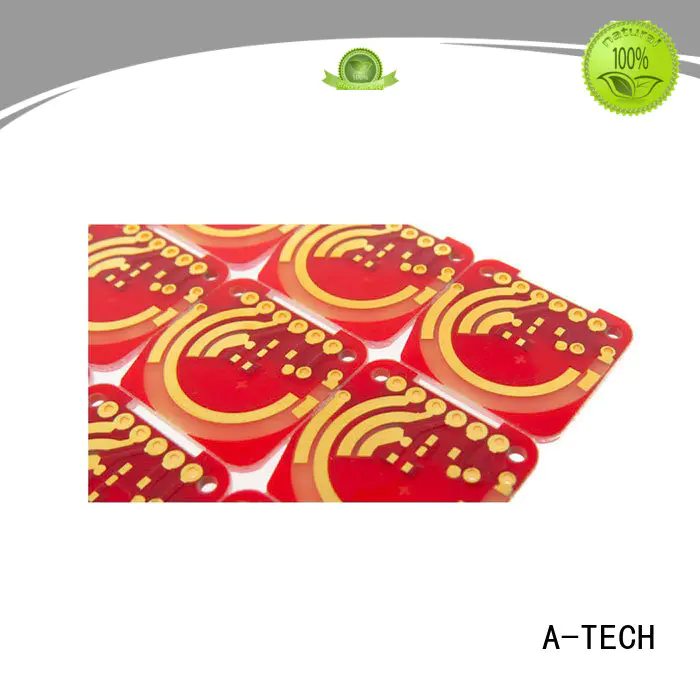
Hard gold plated, the full name is Electrolytic Nickel Electrolytic Gold. The most common application of hard gold plated is edge connectors(gold fingers), and it may also be plated over the entire circuit boards.
Hard Electrolytic gold consists of a layer of gold plated over a barrier coat of nickel. Hard gold is extremely durable, so it is most commonly applied to high-wear areas such as gold fingers and keypads.
Hard gold is not generally applied to solderable areas, because of its high cost and its relatively poor solderability. The maximum thickness that IPC considers to be solderable is 17.8U”, so if this type of gold must be used on surfaces to be soldered, the recommended nominal thickness should be about 5-10U”.
The advantages of hard gold plated
● Hard, Durable surface
● RoHS Compliant
● Long Shelf life
● Excellent for high-wear products
The disadvantages of hard gold plated
● Additional high cost
● Extra complicated manufacturing process
● Etching undercut can lead to slivering/flaking
● Finish does not fully encapsulate trace sidewalls, except in gold finger areas
A-TECH is capable of using hard gold plated on both of gold fingers and the entire PCB, the typical thickness of hard gold plated for gold fingers can be 0.1 – 3.0um, and the typical thickness of hard gold plated on entire board is 0.1 – 1.27um.
Copyright © 2025 A-TECH CIRCUITS Co., Ltd. | All Rights Reserved
Hello, please leave your name and email here before chat online so that we won't miss your message and contact you smoothly.