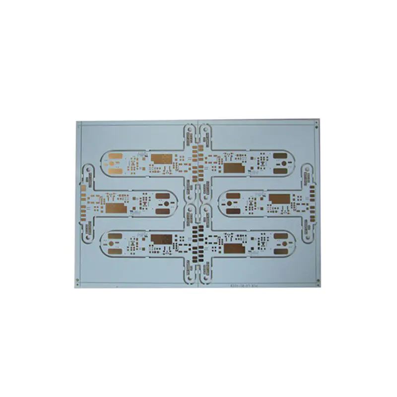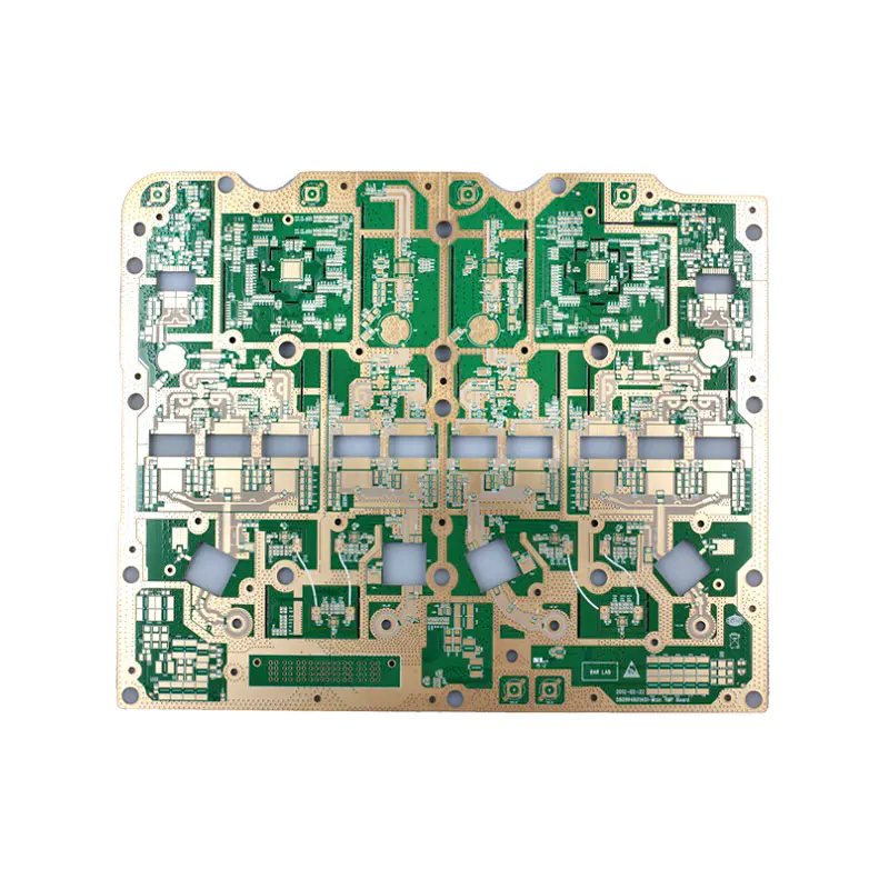
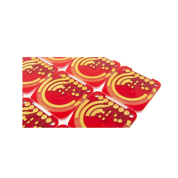
Double-sided PCB
PCB Fabrication
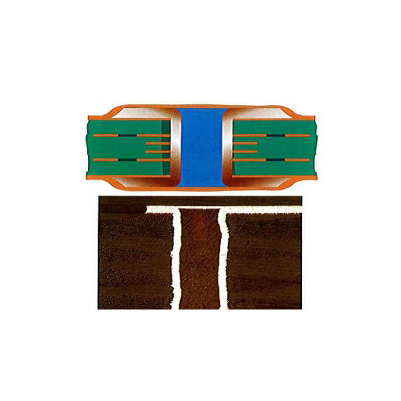
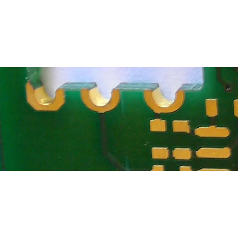
How did A-TECH design edge plating pcb?
2021-04-26
The design process of edge plating pcb can be finished through 4 steps. Concept developing and product design planning come first. Our designers and technicians work together for the expected product performance and appearance design. The detailed design process comes next. Based on the results of the discussion, our designers should consider the materials processing, target application fields, and user experience comprehensively when conducting the product design rather than focusing on the product shapes, colors, and specifications only. Then, designers will deliver the product drawings or sketches to every department of our company for feedback collecting. The last step is the final confirmation. After reaching a mutual agreement on the product design between customers and us, the product design process is finished and the sample will be made based on the design sketches.
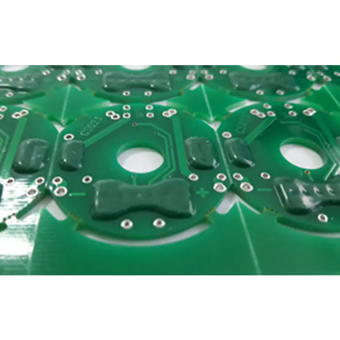
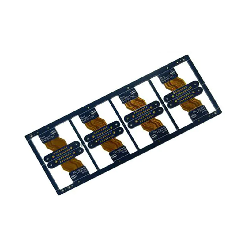
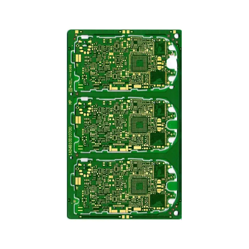
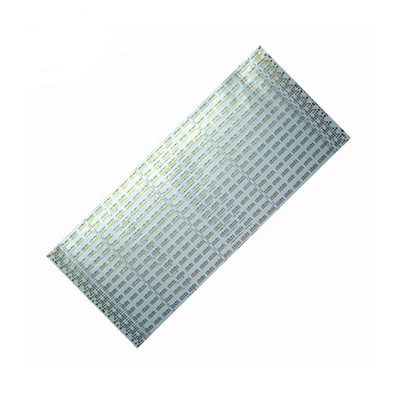
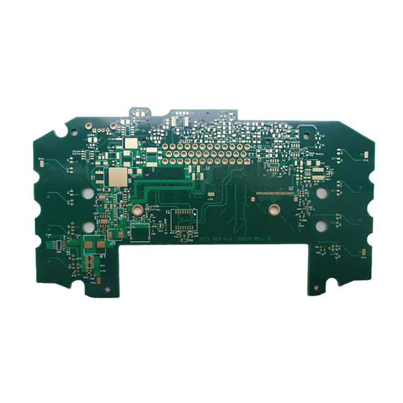
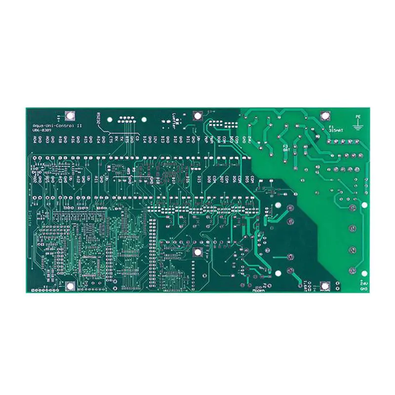
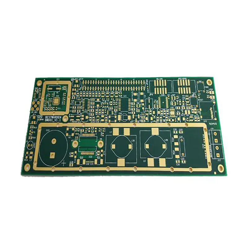
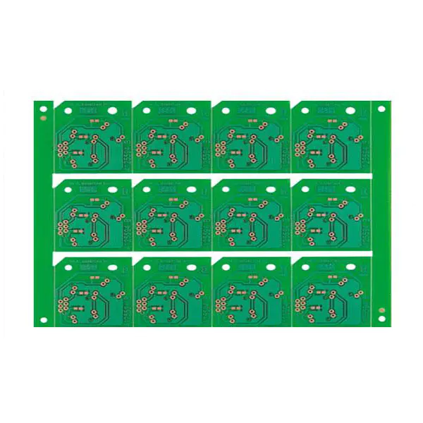
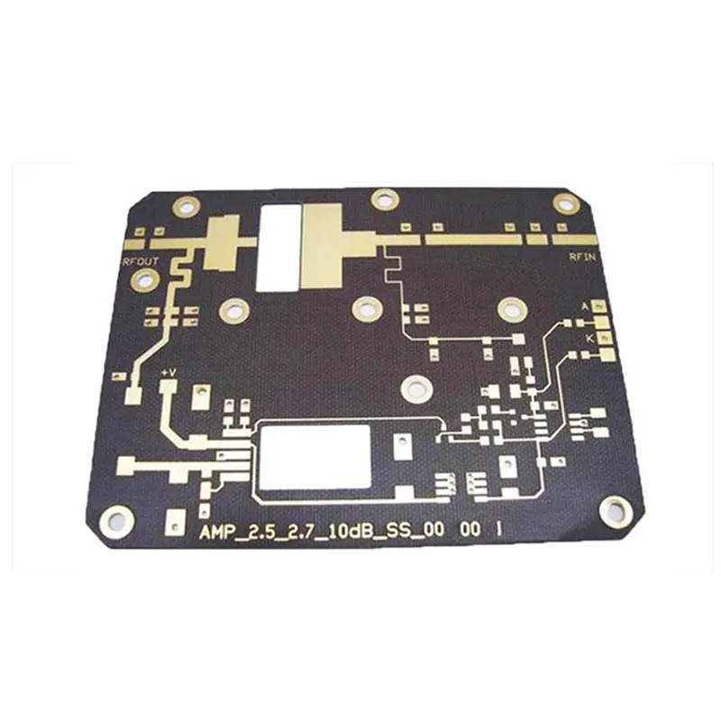
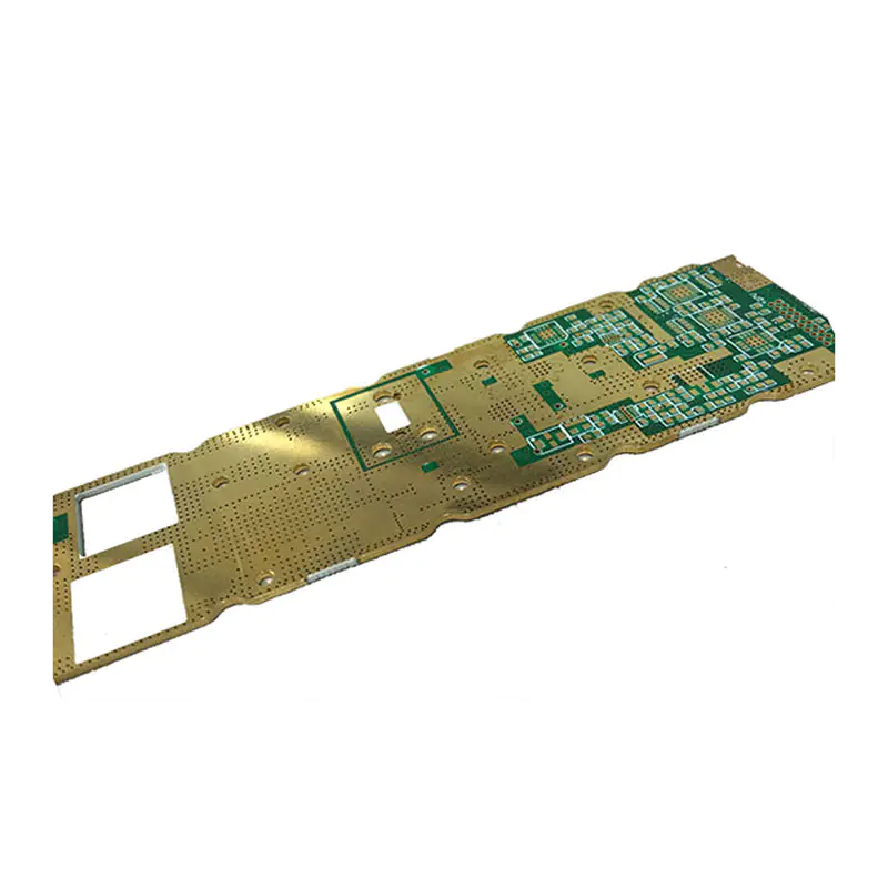
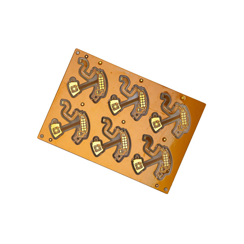
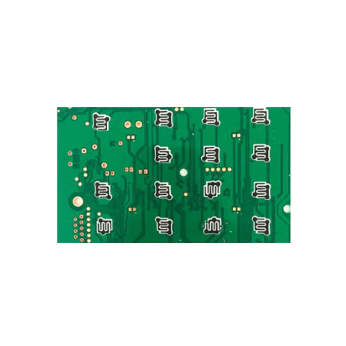
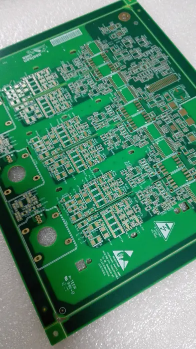
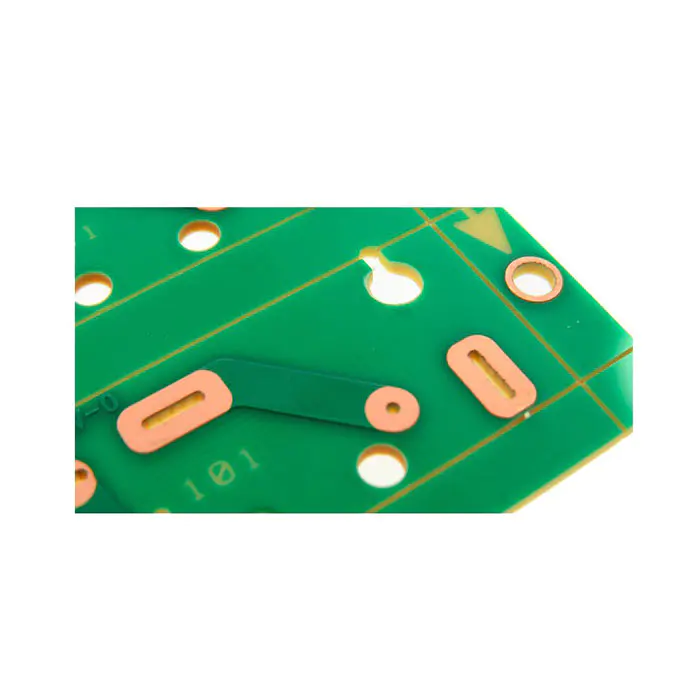
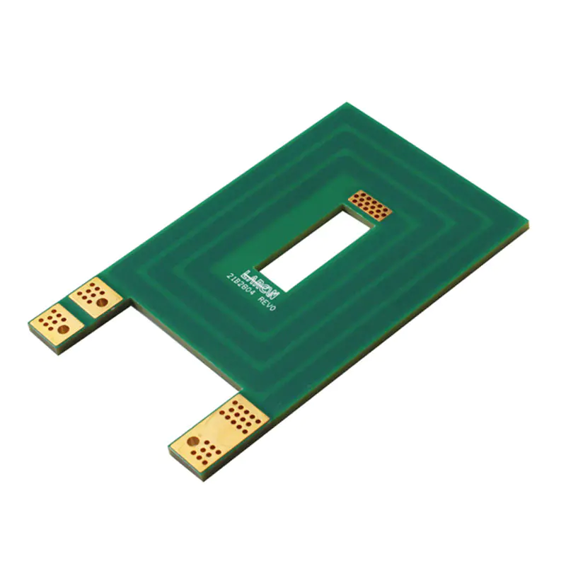
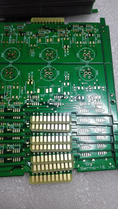
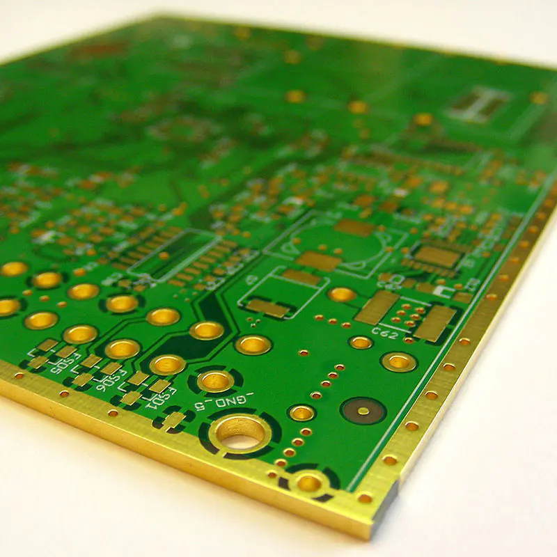
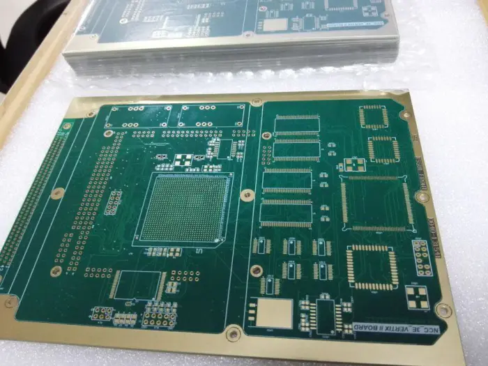
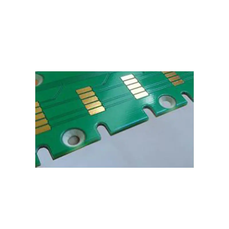
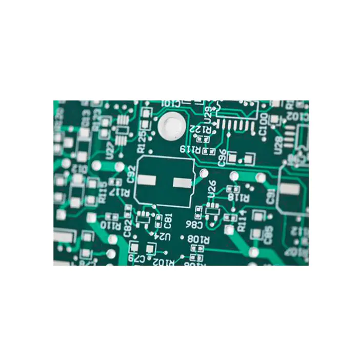
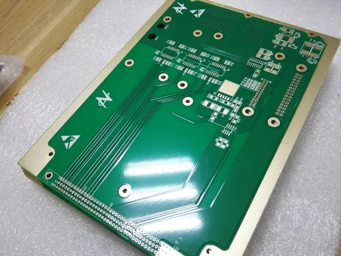
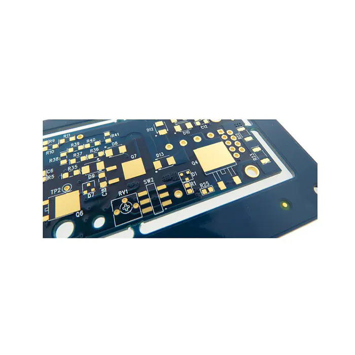
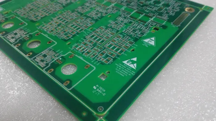
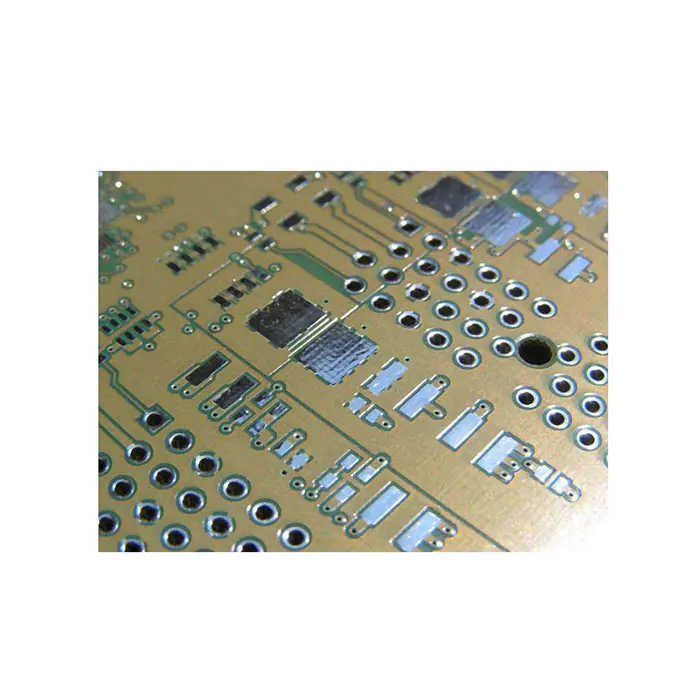
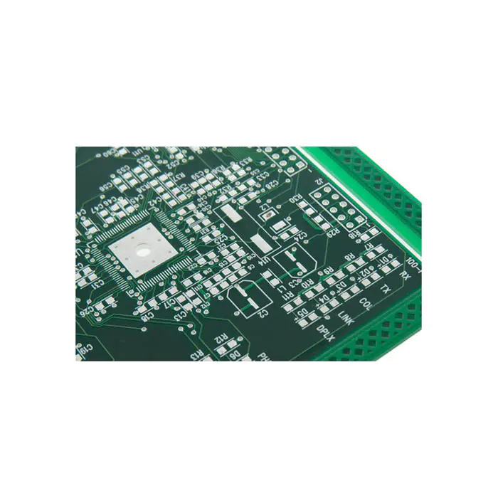
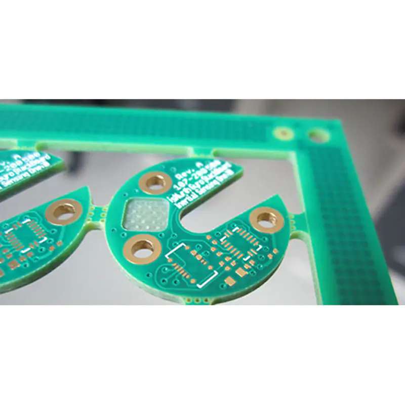
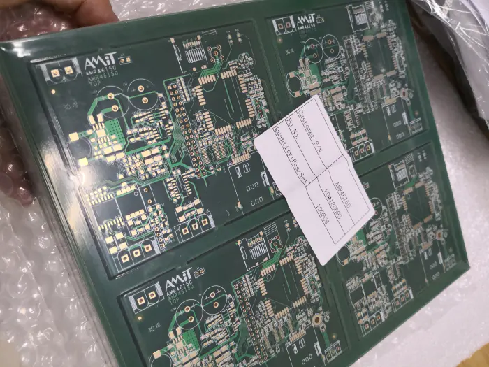
A-TECH CIRCUITS Co., Ltd. deals in PCB Fabrication of fine quality at preferential prices. A-TECH's main products include PCB Fabrication series. The product has a smooth surface without any cracks or holes. It is hard for bacteria, viruses, or other germs to become lodged into it. Being laminated by advanced vacuum lamination equipment, it has a uniform dielectric thickness after lamination. The product has won numerous praises for its outstanding characteristics. It is extremely popular in the markets of Europe, North America, and Asia.
Our company engages in sustainable management. We periodically discuss strategies in order to accurately grasp changes in social demands from the international community and reflect them into management from a long-term perspective.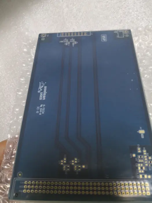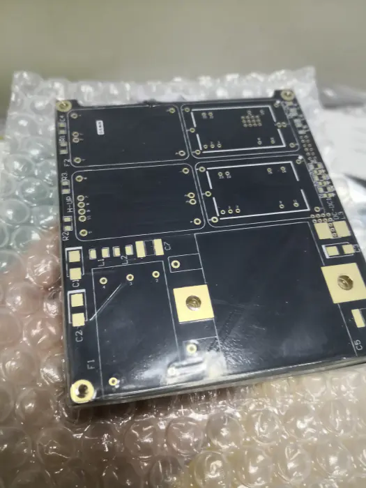
Custom message
Related Products