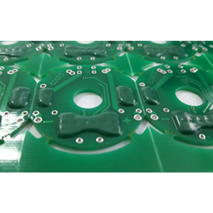
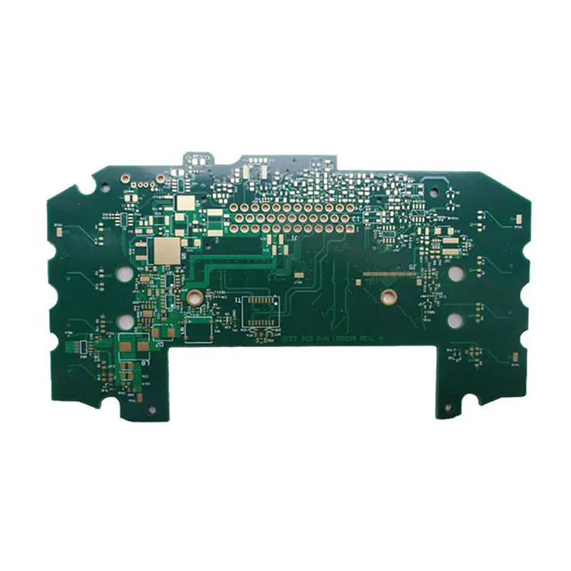
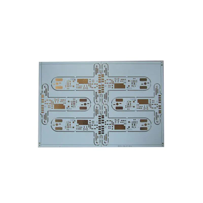
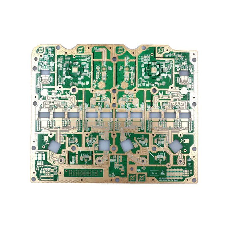
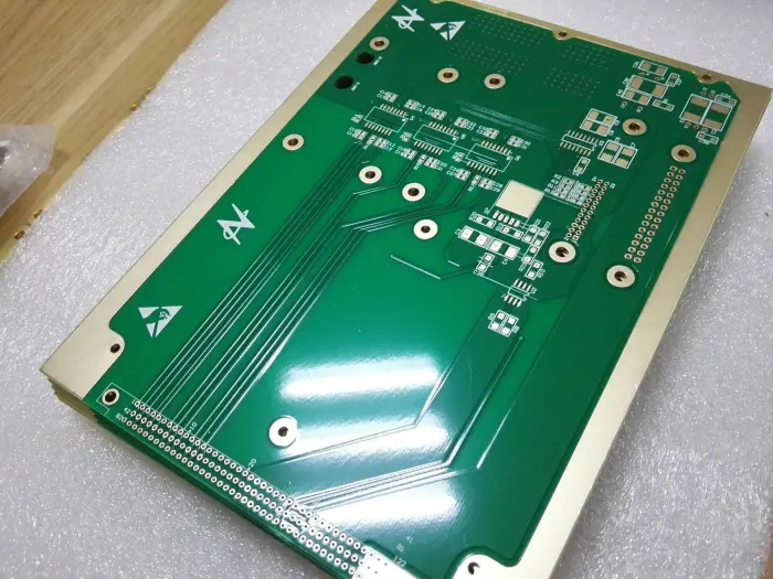
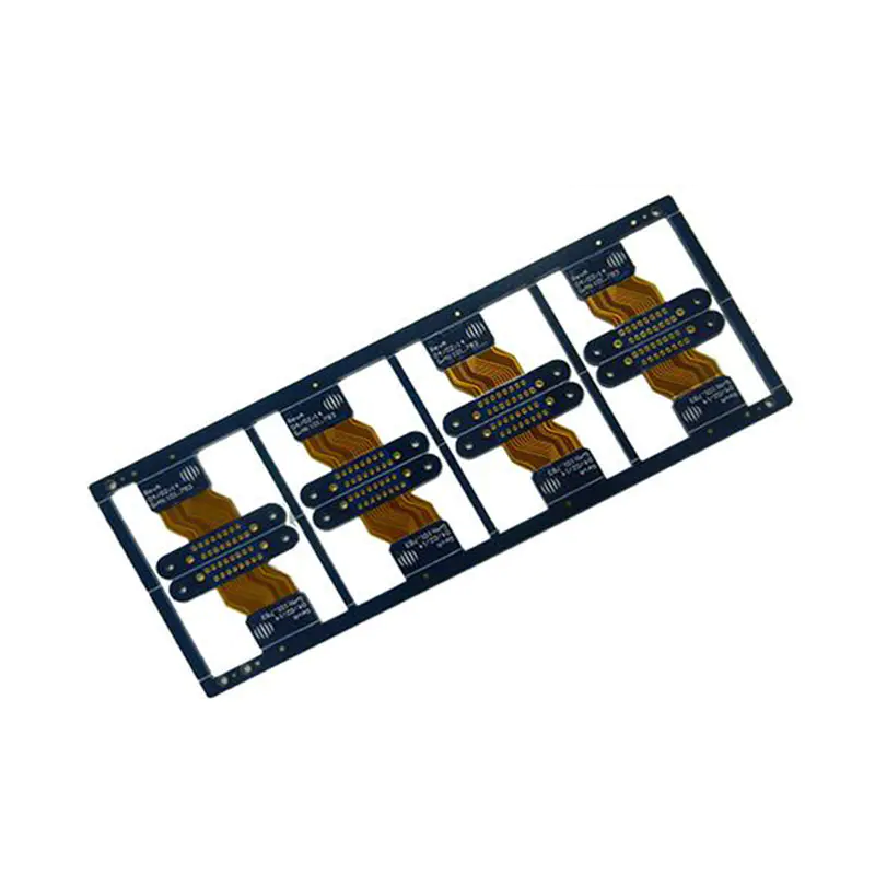
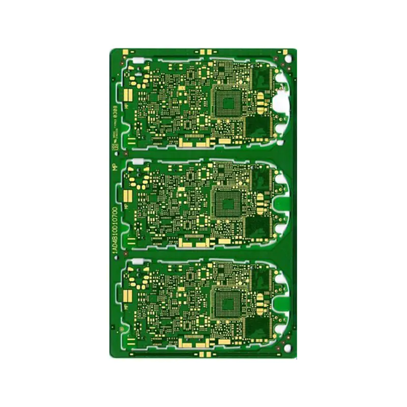
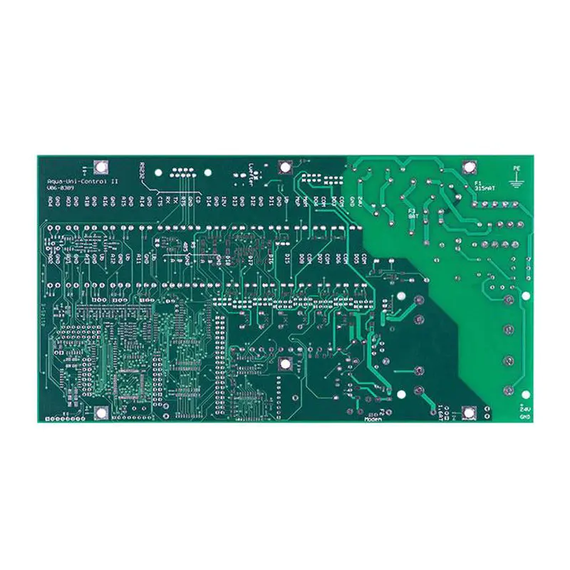
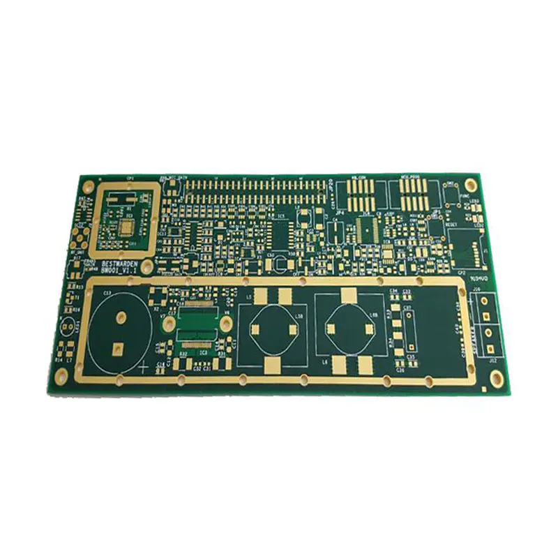
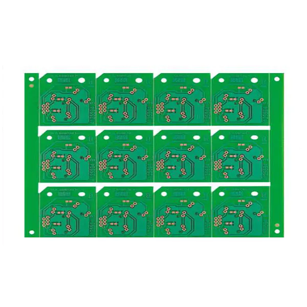
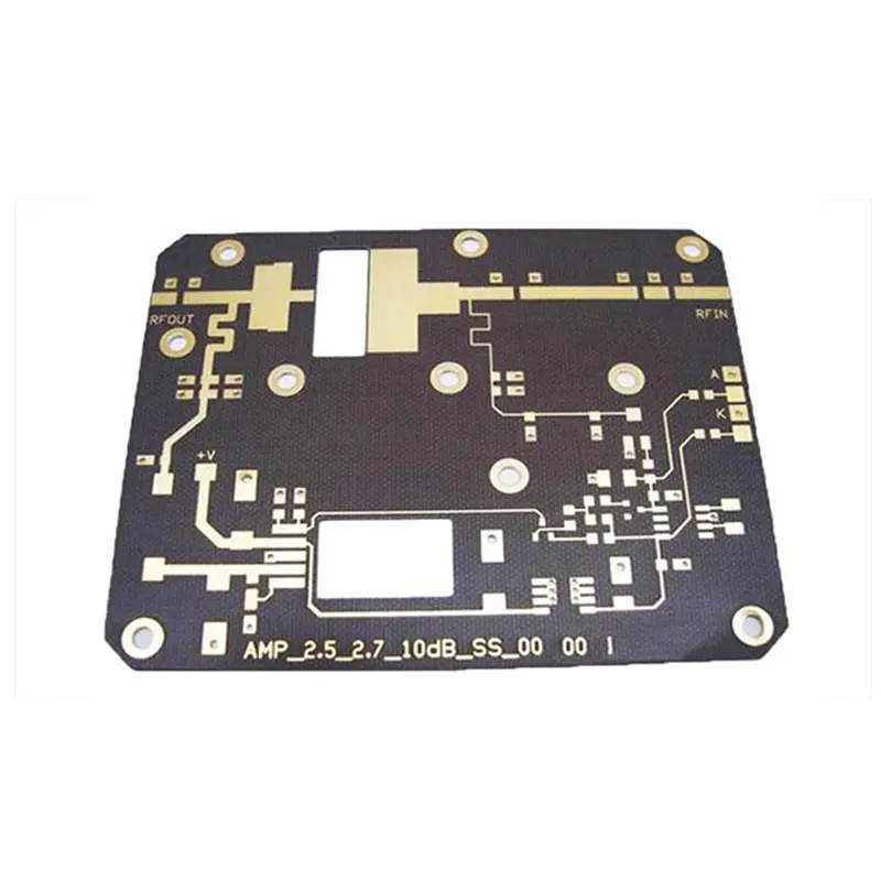
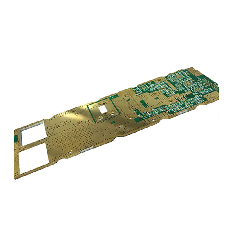
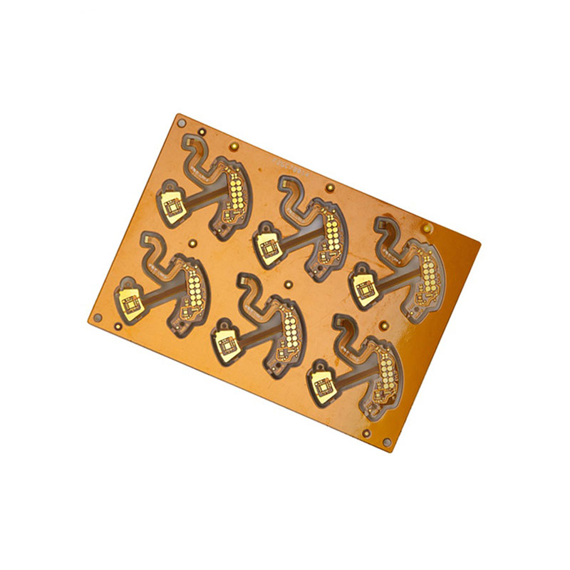
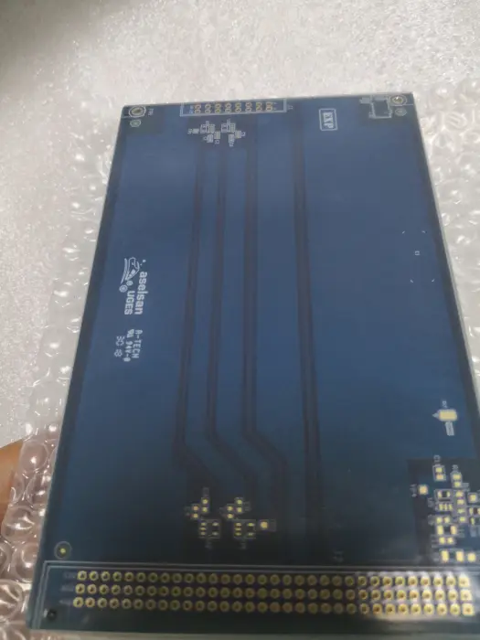
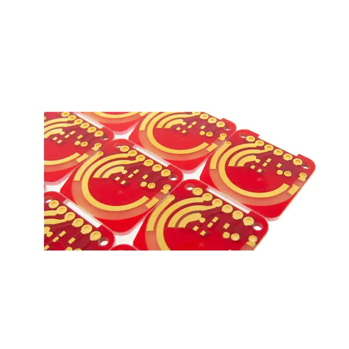
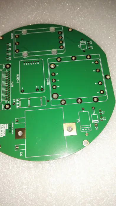
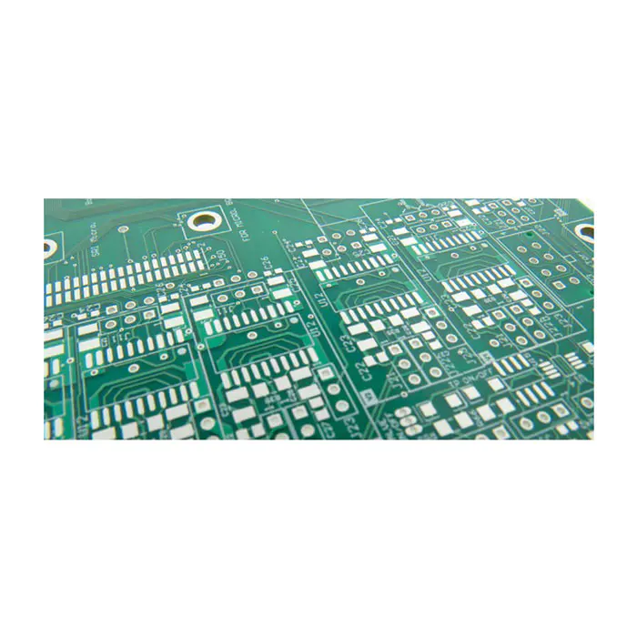
loading

Home  > Buy PCB MANUFACTURING  > Pcb Surface Finish Exporter  >  hasl pcb finish leveling for wholesale A-TECH
hasl pcb finish leveling for wholesale A-TECH

hasl pcb finish leveling for wholesale A-TECH

Thickness
0.1-1.27um
Shelf Life
12 Months
Solderability
Good
RoHS Compliant
Yes
Additional Cost
Yes
Supply Capacity
2000 ㎡/Month
Certifications
UL, ISO9001, TS16949
Payment Terms
T/T, Paypal, WU etc.
Shipment Terms
EXW, FOB, DDU etc.
Test Way
100% E-Test
Standard
IPC CLASS 2 / CLASS 3
Price
Get Latest Price
Get the latest price
Quantity Needed:
Pieces
E-mail:
Captcha

Loading verification code...

Please complete verification first

Enterprise Strength
  • A-TECH strictly insists on the service concept to be demand-oriented and customer-oriented. We are committed to providing all-round services for consumers to meet their different needs.
Product Comparison
Under the guidance of market, A-TECH constantly strives for innovation. PCB Manufacturing has reliable quality, stable performance, good design, and great practicality.A-TECH's PCB Manufacturing has more advantages over similar products in terms of technology and quality.
Company Advantages
1. The design of A-TECH hasl pcb finish involves several considerations, including overall bag weight, overall shape and balance, materials used in construction, and type and configuration of zippers.
2. The product features enough traction. The outsole effectively makes contact with the ground and the grooves and treads can help maintain traction.
3. The product can withstand extremely high temperatures. The wood materials used do not easily warp when subjected to extreme conditions.
4. A-TECH CIRCUITS Co., Ltd. has provided great value to hasl pcb field.
5. A high standard hasl pcb production base has been established by A-TECH CIRCUITS Co., Ltd..


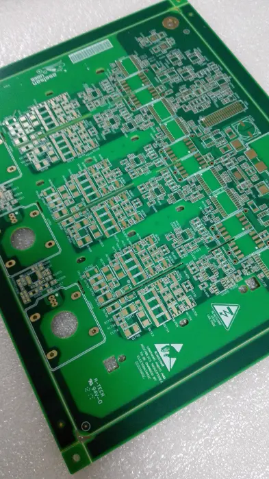
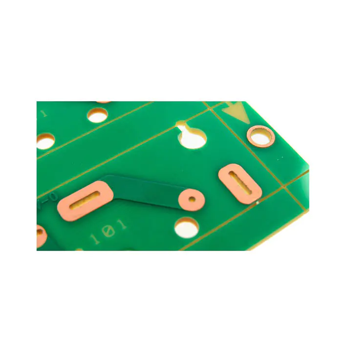
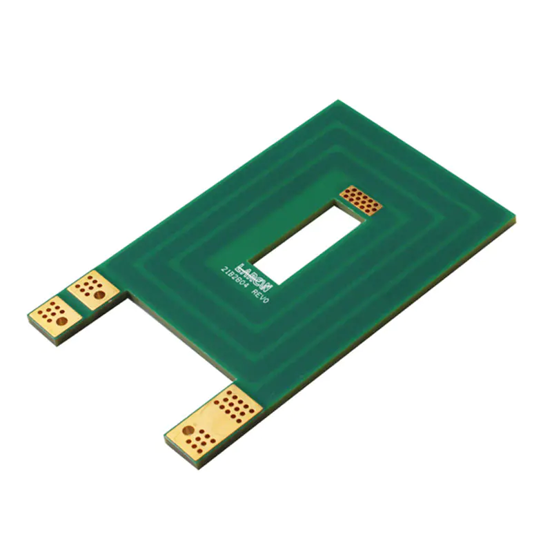
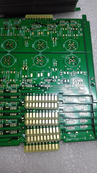
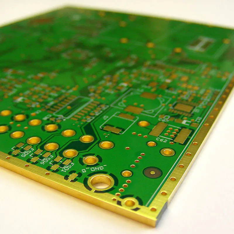
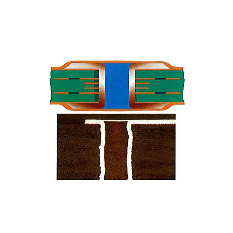
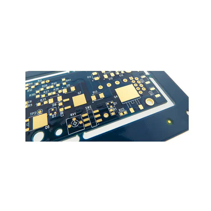
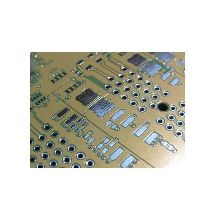
Hard gold plated, the full name is Electrolytic Nickel Electrolytic Gold. The most common application of hard gold plated is edge connectors(gold fingers), and it may also be plated over the entire circuit boards.

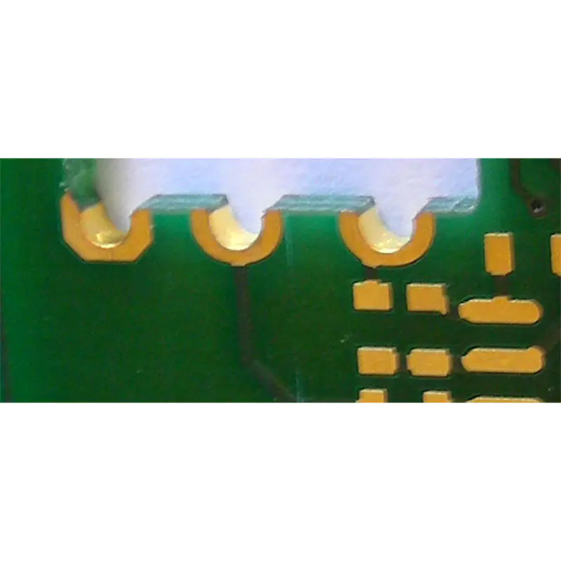
Hard Electrolytic gold consists of a layer of gold plated over a barrier coat of nickel. Hard gold is extremely durable, so it is most commonly applied to high-wear areas such as gold fingers and keypads.

Hard gold is not generally applied to solderable areas, because of its high cost and its relatively poor solderability. The maximum thickness that IPC considers to be solderable is 17.8U”, so if this type of gold must be used on surfaces to be soldered, the recommended nominal thickness should be about 5-10U”.


The advantages of hard gold plated

● Hard, Durable surface
● RoHS Compliant
● Long Shelf life
● Excellent for high-wear products


The disadvantages of hard gold plated

● Additional high cost
● Extra complicated manufacturing process
● Etching undercut can lead to slivering/flaking
● Finish does not fully encapsulate trace sidewalls, except in gold finger areas


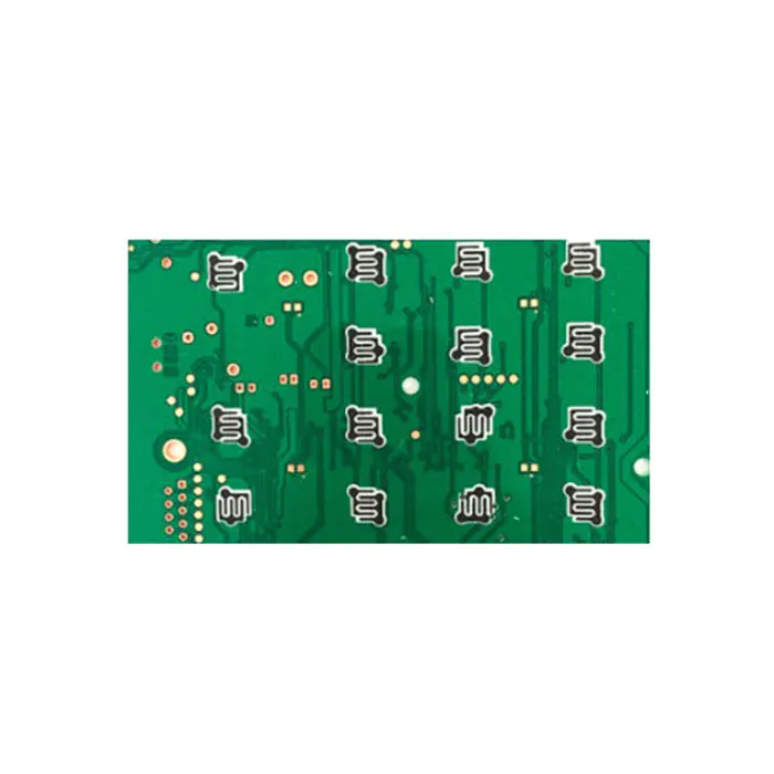
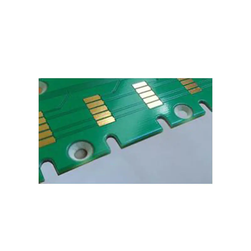
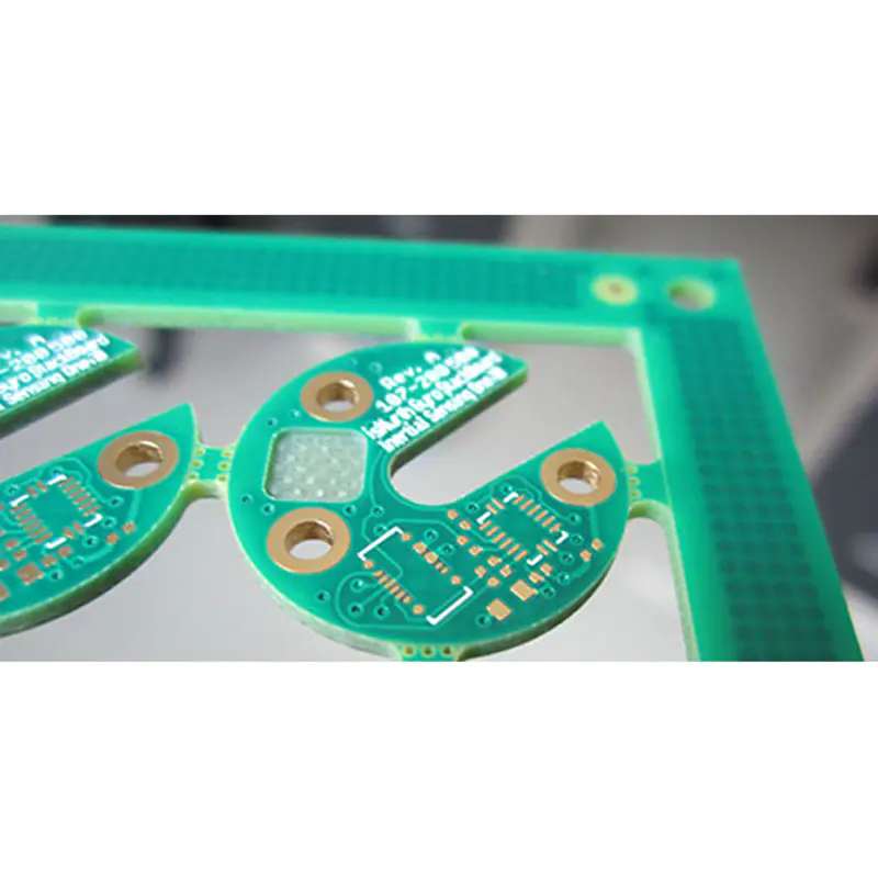
A-TECH is capable of using hard gold plated on both of gold fingers and the entire PCB, the typical thickness of hard gold plated for gold fingers can be 0.1 – 3.0um, and the typical thickness of hard gold plated on entire board is 0.1 – 1.27um.


Company Features
1. A-TECH has made achievements in the field of hasl pcb .
2. By virtue of solid technical foundation, A-TECH CIRCUITS Co., Ltd. becomes forefront in immersion tin pcb industry.
3. A-TECH CIRCUITS Co., Ltd. also do repairs and maintenance of immersion gold pcb . Inquire online! A-TECH presents you with the best pcb mask. Inquire online! A-TECH CIRCUITS Co., Ltd. will stick to using the first-class technology, first-class management, first-class products and first-class service to return customer. Inquire online! The tight network of sales and service training stations of A-TECH CIRCUITS Co., Ltd. makes it easier to provide customers with more convenient services. Inquire online!
Product Message

Loading verification code...

Please complete verification first

Chat Online 编辑模式下无法使用
Chat Online inputting...
Please hold on and we will get back to you soon