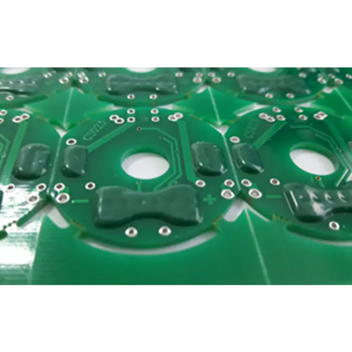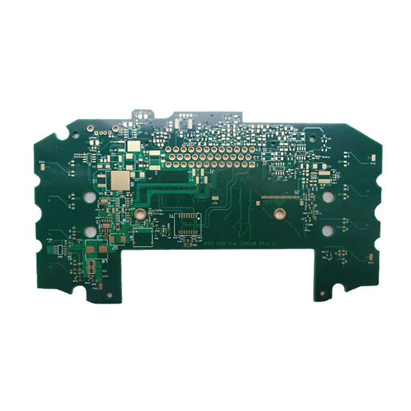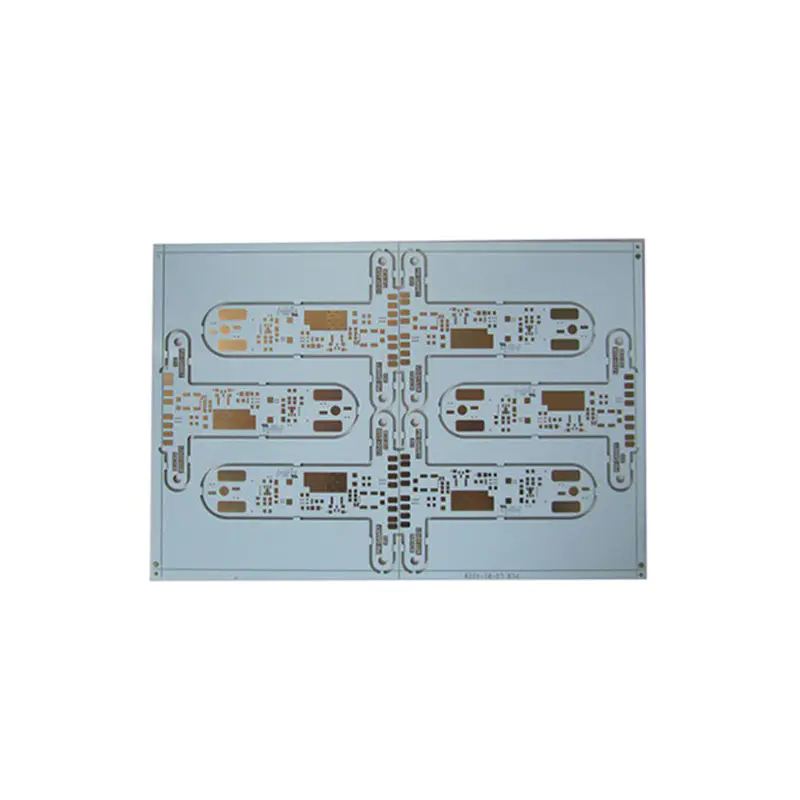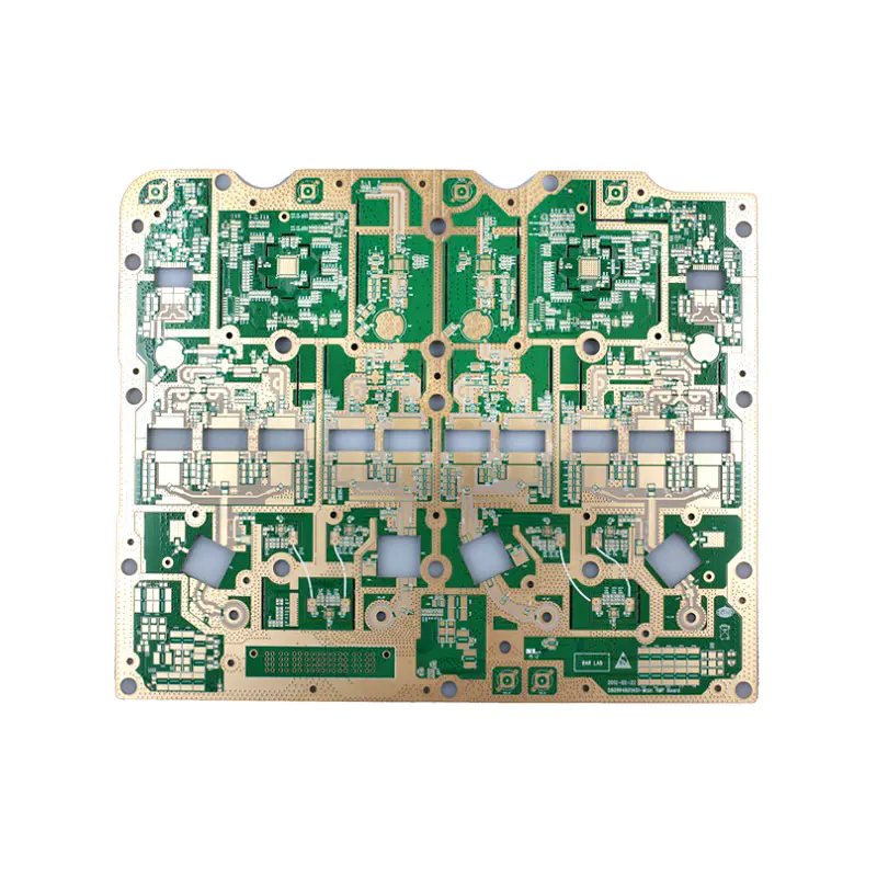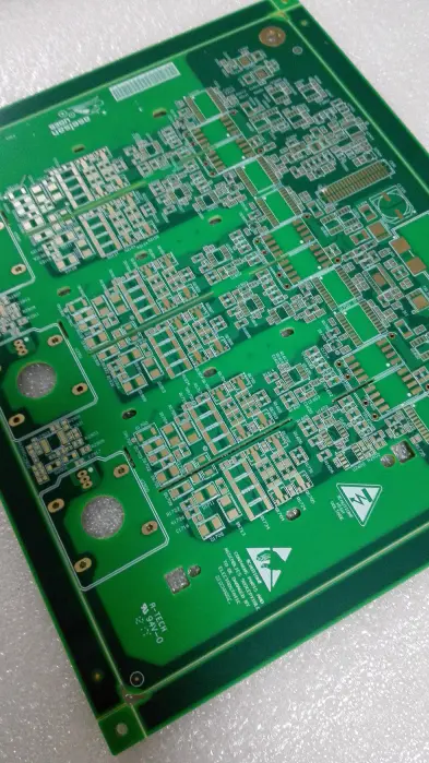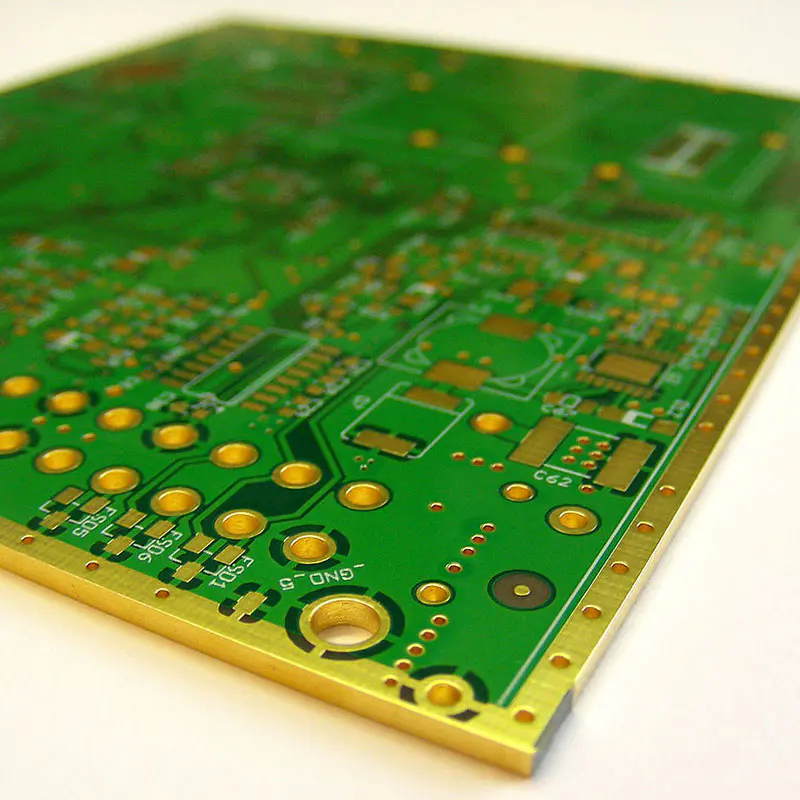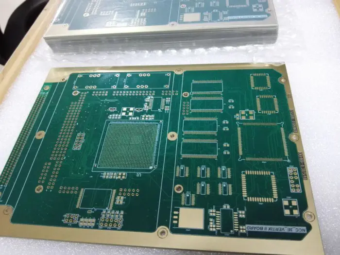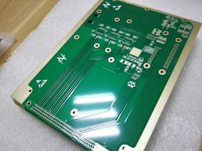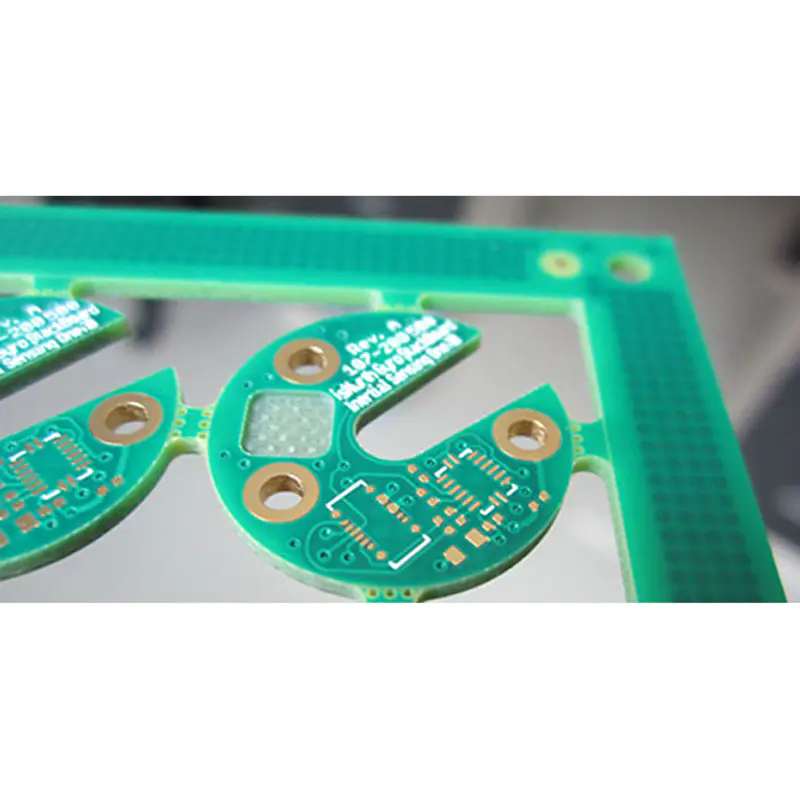
Double-sided PCB
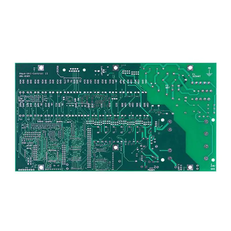
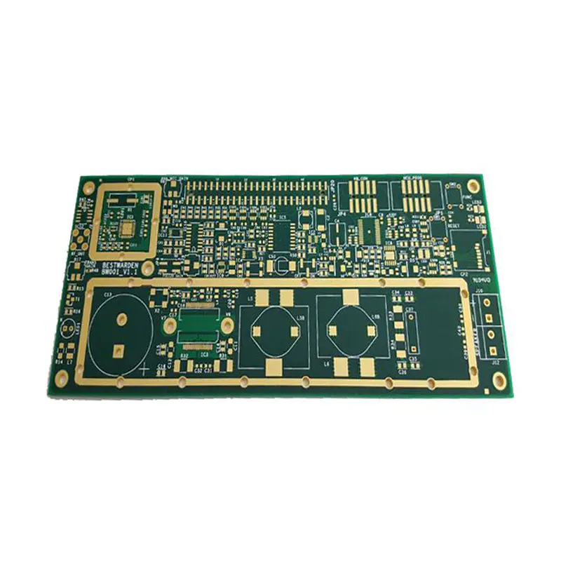
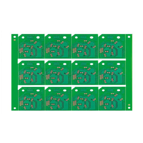
Related Products


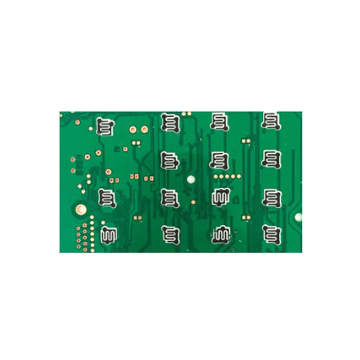
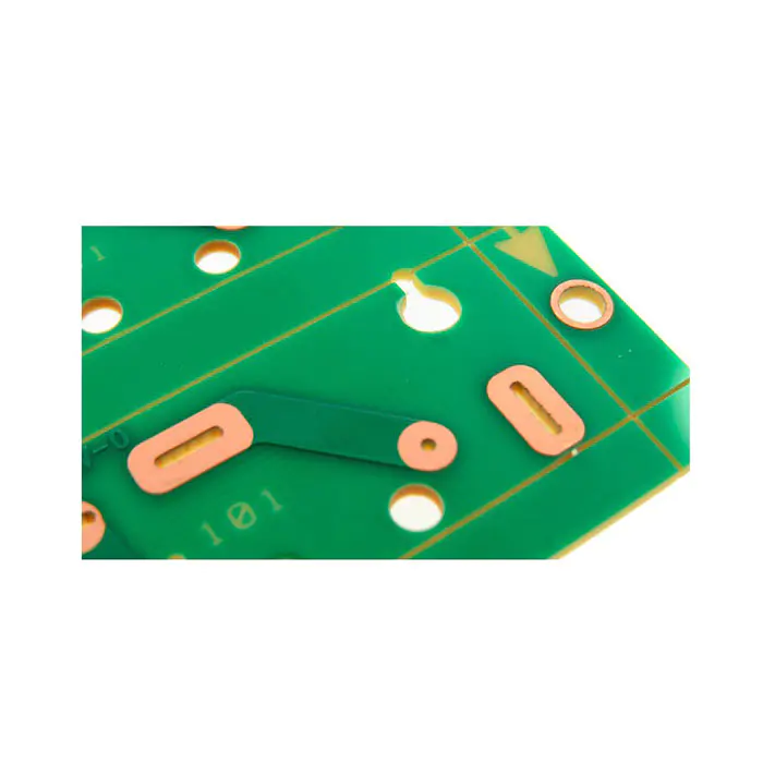
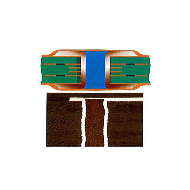
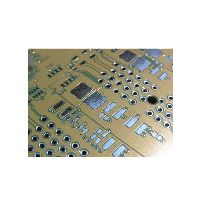
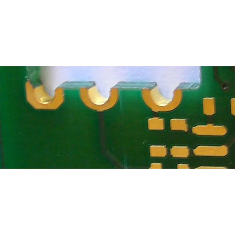
Carbon Ink is typically used to create a protective contact surface for switches, sometimes few copper elements or patterns of the PCB board are used for keyboard contacts, LCD contacts and jumpers etc, to do this it’s usable to print some conductive/resistive carbon ink over those copper part, which normally are SMD pads or fingers or other typical contact patterns.
Carbon Ink printing process is screen printing like silk screen process, the carbon ink is printed in the specified location of the PCB, after oven cured and tested, formed a carbon film which with certain resistance to instead of the original resistance components. The difference is that silkscreen is only played a welding role but carbon ink has conductive performance.
The typical thickness of carbon ink is 10-50um, because the carbon ink has good electrical conductivity, so the carbon printed on the finished PCB should have a certain gap to ensure that no short circuits, usually require the min 8mil gap for Hoz copper and min 12mil gap for 1-3oz copper, and the minimum carbon line width is 12mil.
A-TECH is a capable PCB manufacturer to offer Carbon ink process, we require the data files to clearly indicate on which side of the PCB carbon is to be applied and the carbon areas must be properly indicated on specific layers with proper file naming.
General inquiries & Customer Service
Tel: 86-755-2335 9039 | Fax: 86-755-3318 0939
E-Mail: Enquiry@atechcircuit.com
Skype: atechcircuits

Headquarters: 602, Building B3, Zhimei Huizhi Industrial Park, Fuyong Street, Bao'an District, Shenzhen City, China
Copyright © 2025 A-TECH CIRCUITS Co., Ltd. | All Rights Reserved
Hello, please leave your name and email here before chat online so that we won't miss your message and contact you smoothly.