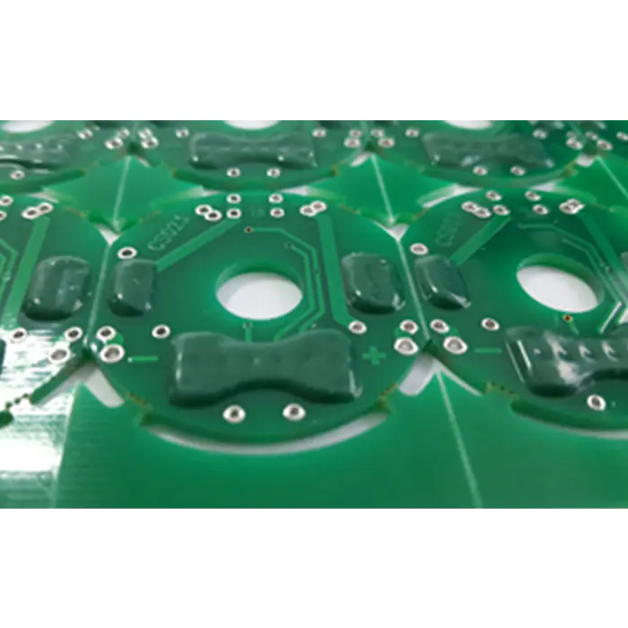
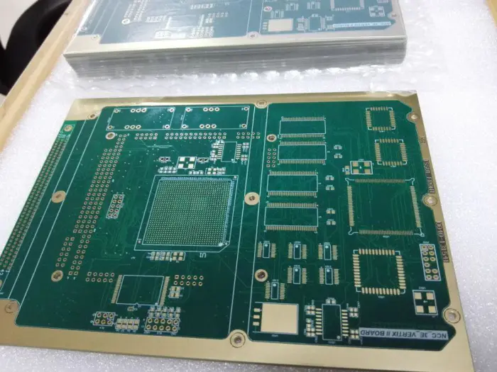
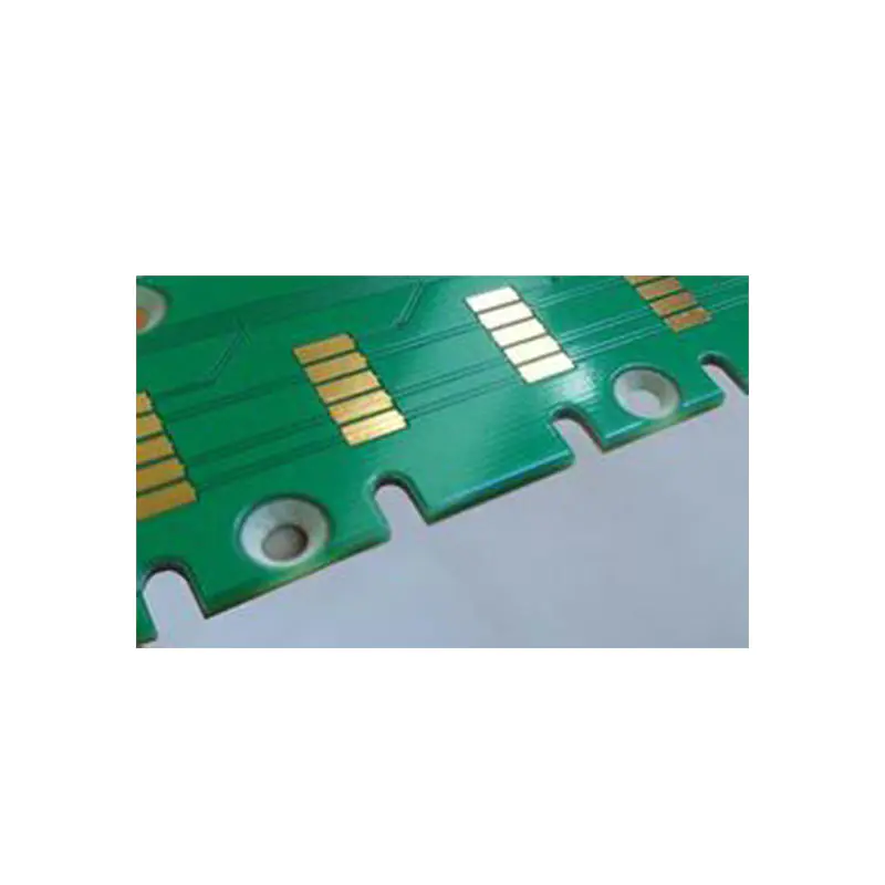
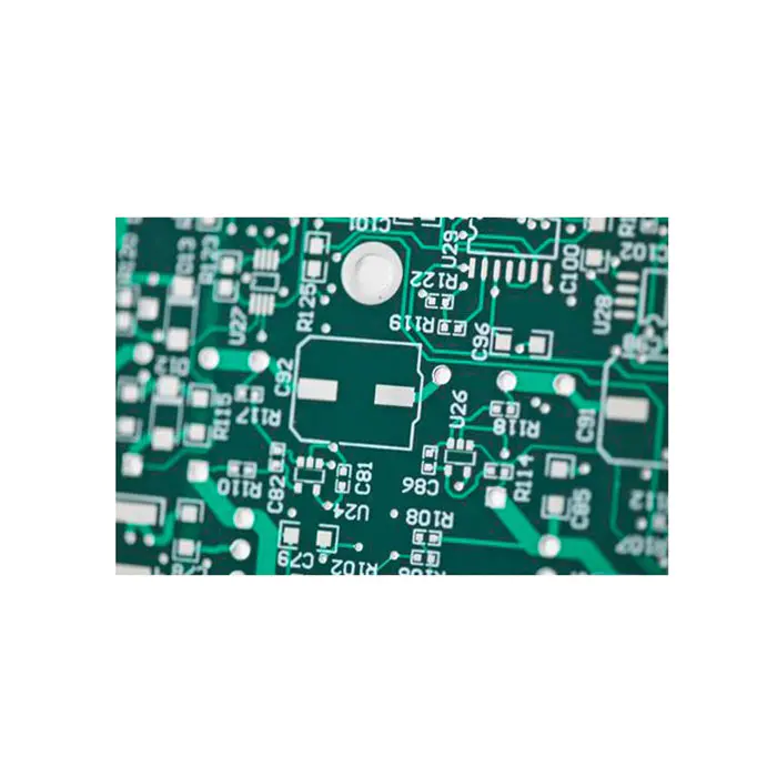
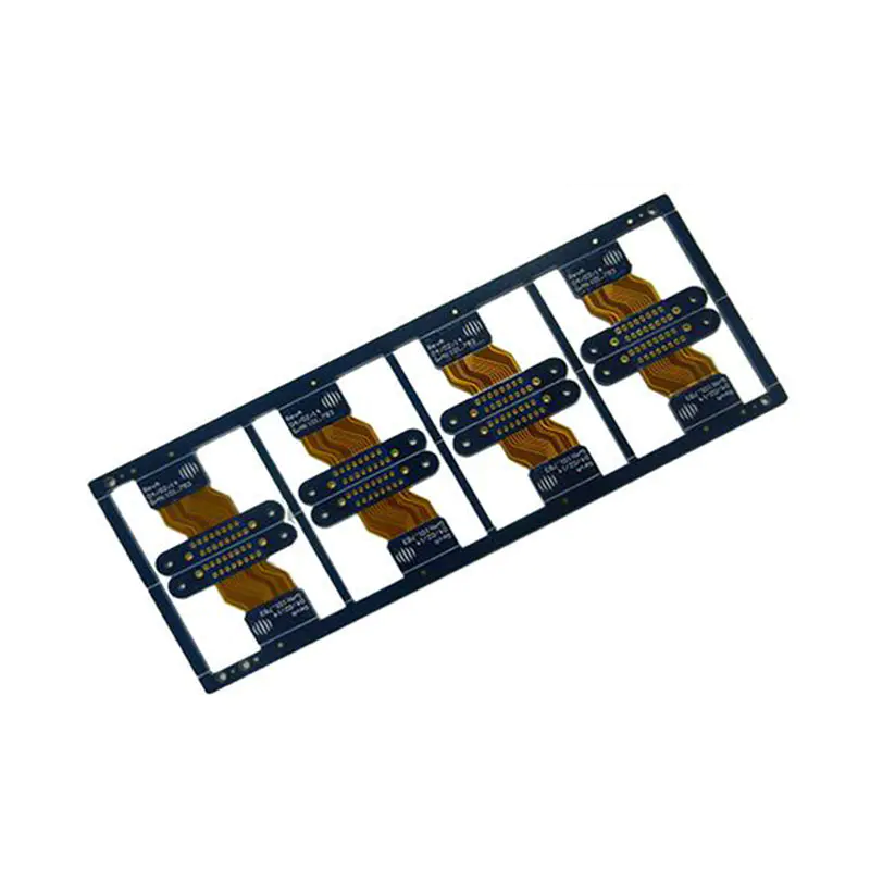
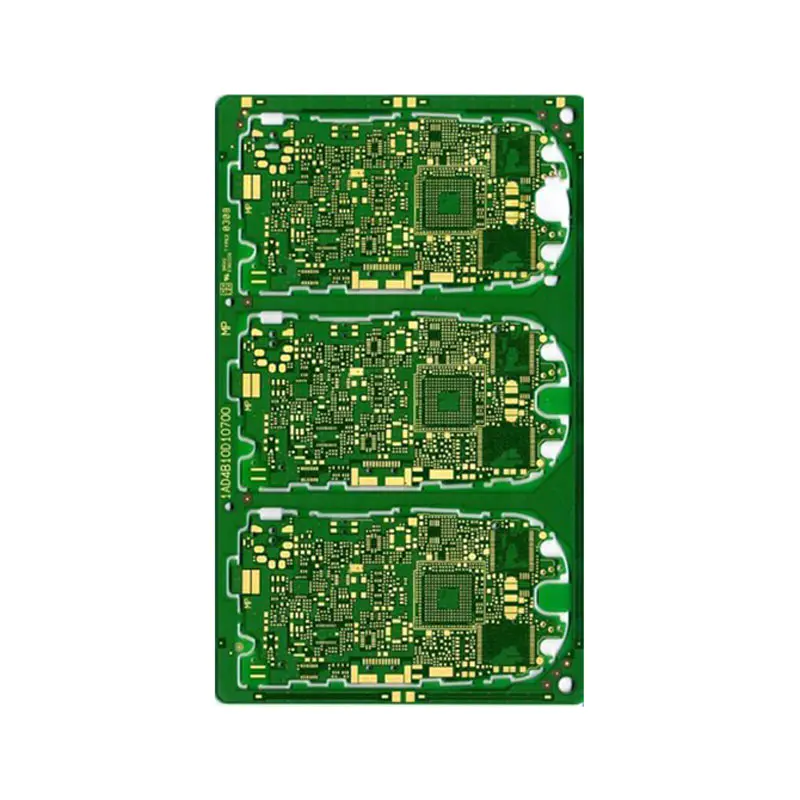
loading

Home  > Buy PCB MANUFACTURING  > Pcb Special Technology Factory  >  buried edge plating pcb best price for wholesale
buried edge plating pcb best price for wholesale

buried edge plating pcb best price for wholesale

Type of Blind Vias
Laser Drill & Mechanical Drill
Min Laser drill blind Vias
0.1mm
Min Mechanical drill blind vias
0.15mm
Min Buried Vias
0.15mm
Min Order Quantity
No
Production Lead Time
6-20 Working Days
Supply Capacity
3000 ㎡/Month
Certifications
UL, ISO9001, TS16949
Payment Terms
T/T, Paypal, WU etc
Shipment Terms
EXW, FOB, DDU etc.
Test Way
100% E-Test
Standard
IPC CLASS 2 / CLASS 3
Price
Get Latest Price
Get the latest price
Quantity Needed:
Pieces
E-mail:
Captcha

Loading verification code...

Please complete verification first

Company Advantages
1. Our edge plating pcb is professionally designed. It can be manufactured with a customized thickness
2. This product has garnered significant attention and praise in the industry. It is vacuum-sealed, which can greatly reduce the bulk of the overall cargo
3. This product is translucent as a whole. The woven base cloth combined with the appropriate coating allows a suitable light transmission value. The product can be resistant to corrosion
4. The electromagnetic compatibility of this product is under reasonable control. It is ensured that it does not generate, or is not affected by electromagnetic disturbance. It is widely used in different electronics industries, such as telecommunication and consumer electronics
5. The product features a stable and robust structure. All of the electric components are sophisticatedly soldered and sealed inside the housing. Hence, they are not affected by external factors. It is offered with low dielectric loss


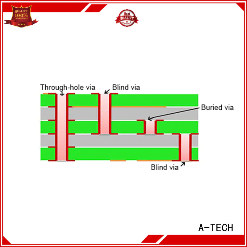
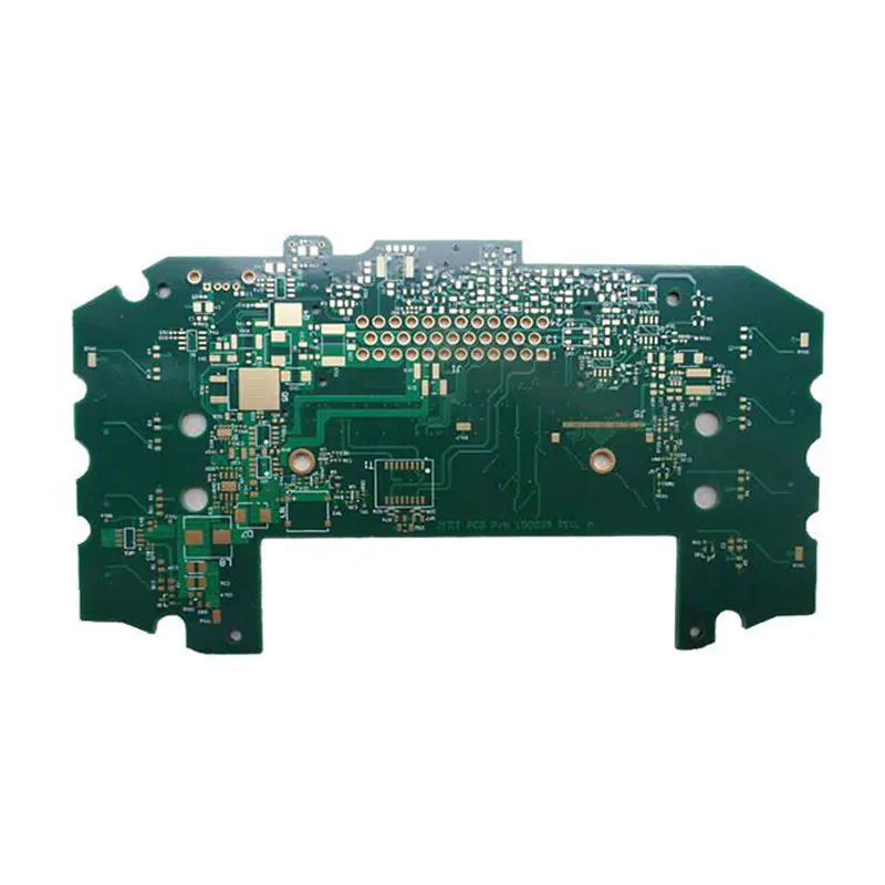
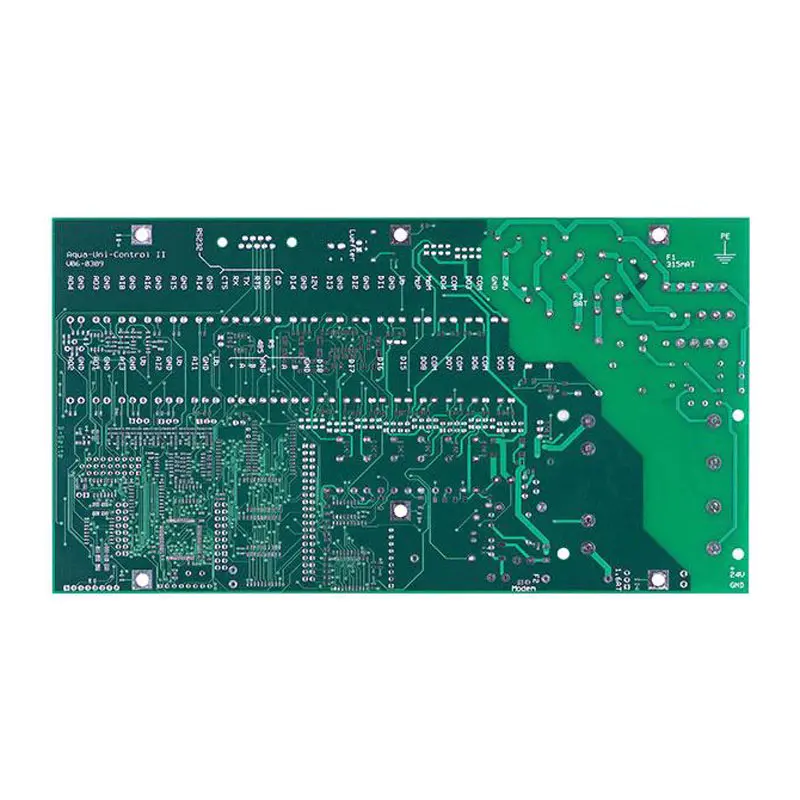
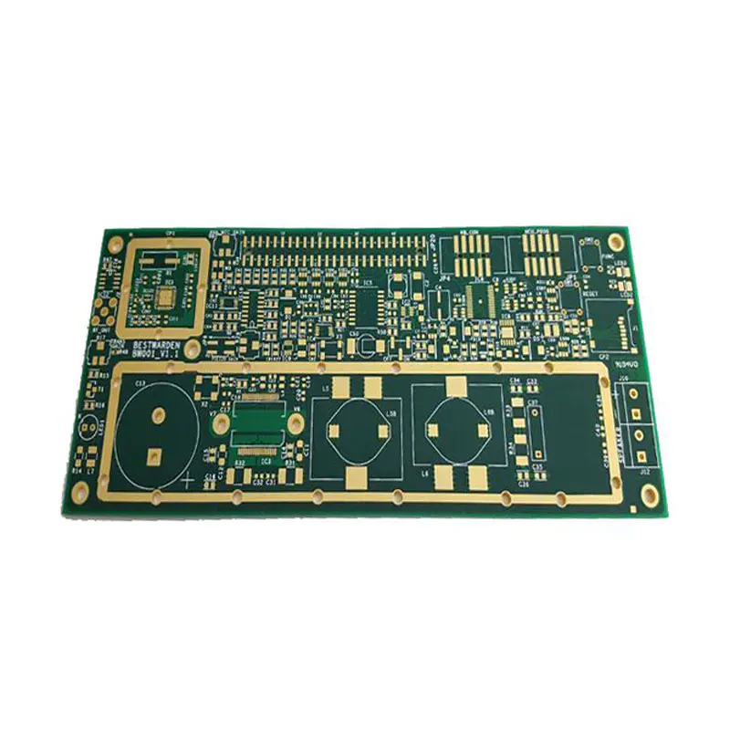
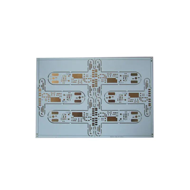
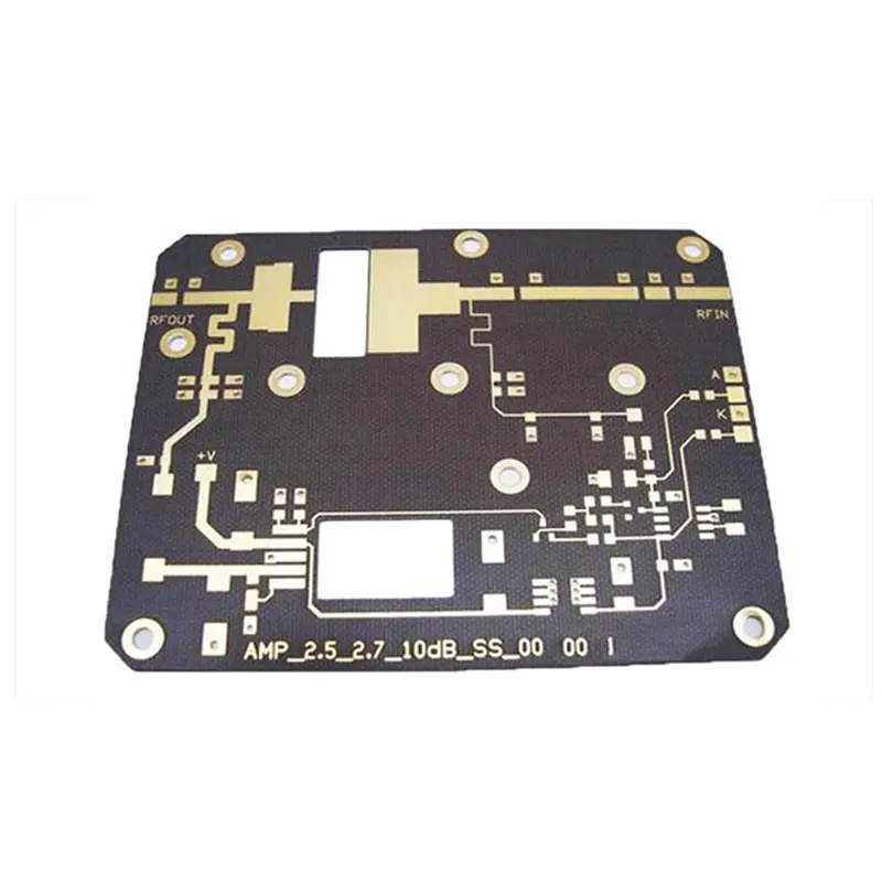
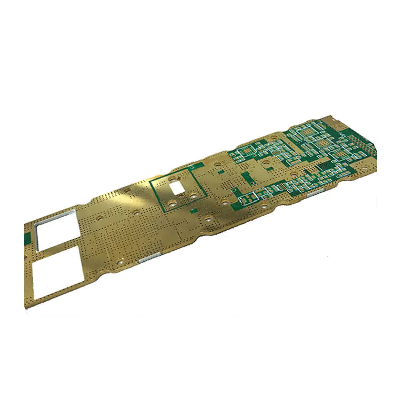
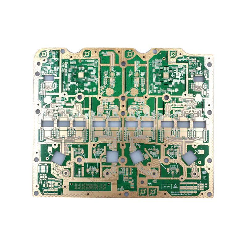
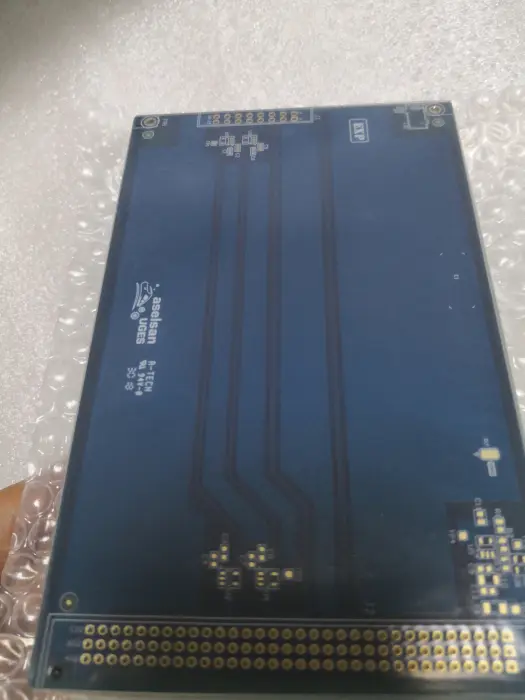
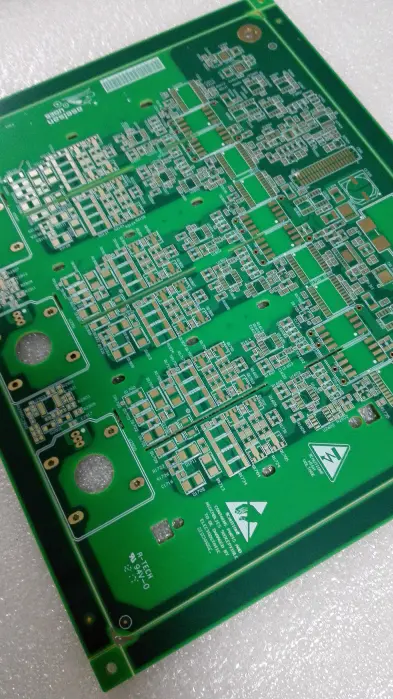
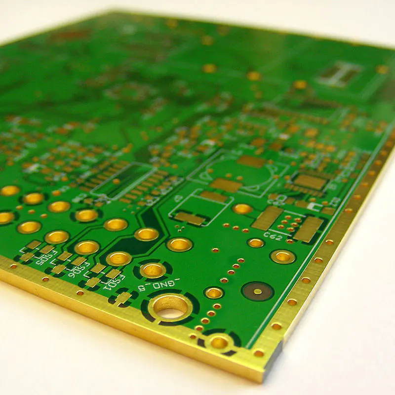
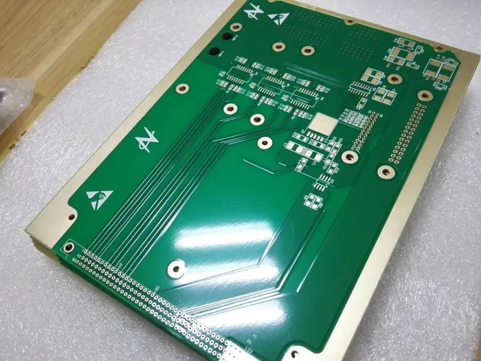
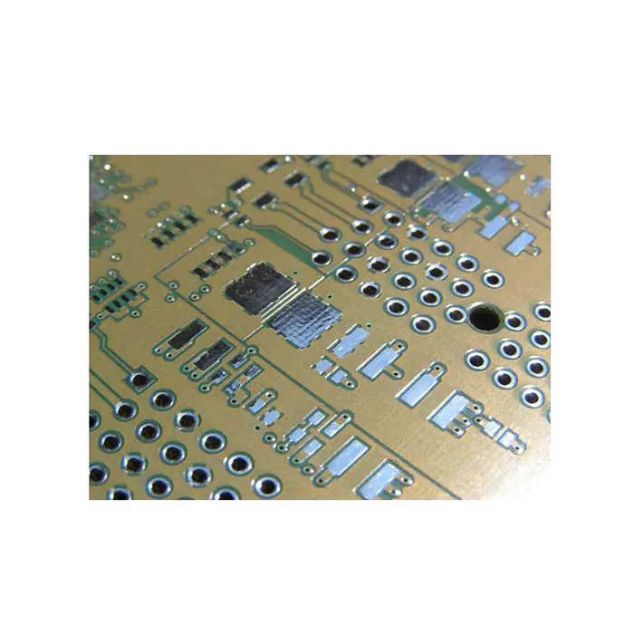
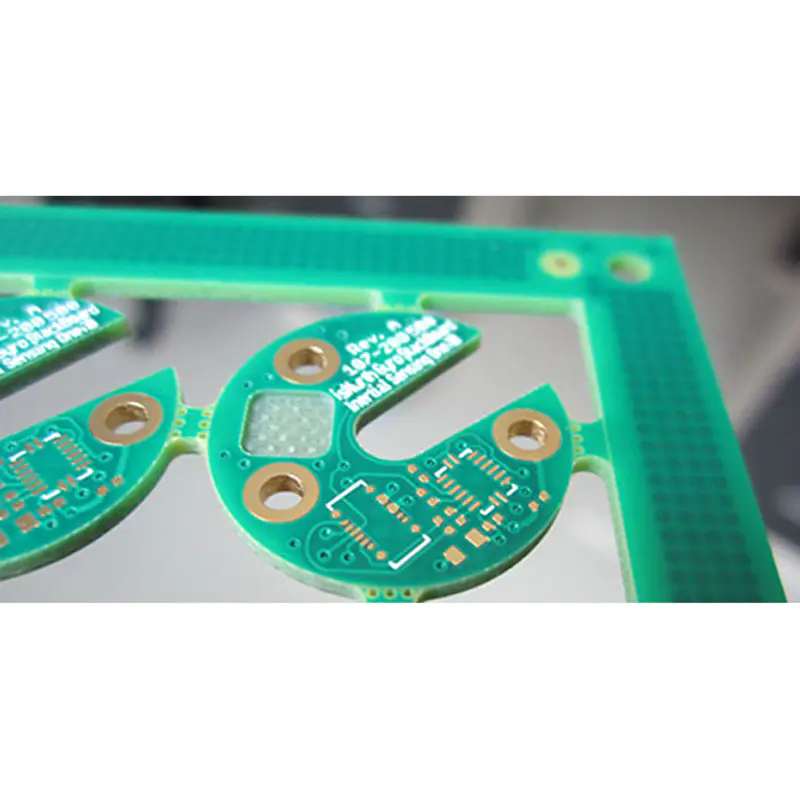
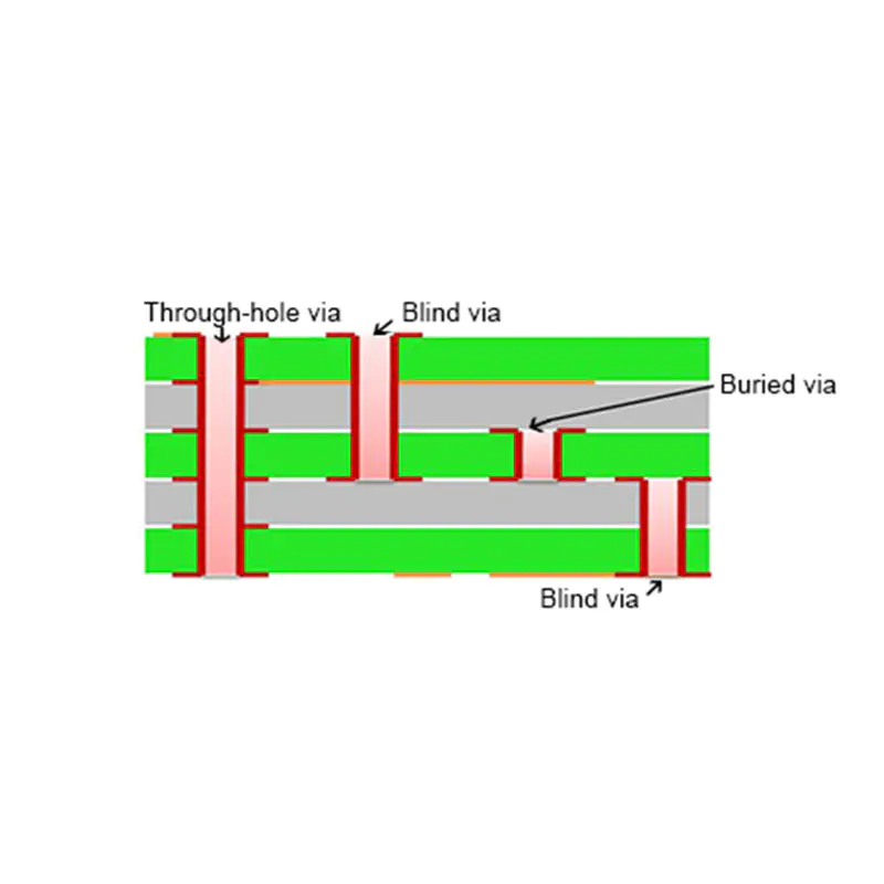
PCB with Blind and Buried Vias

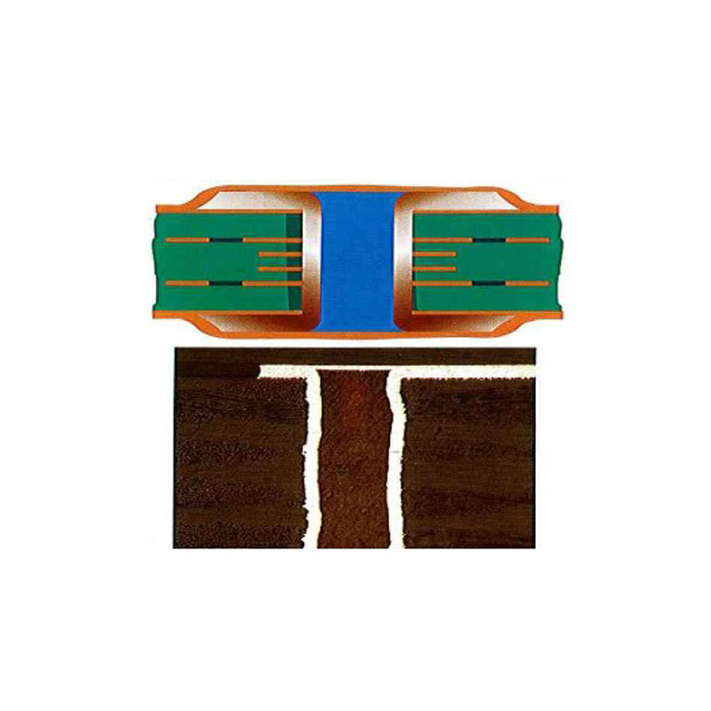
Basically the blind and buried vias are popular to be designed on high density PCBs due to the limit of small space, the blind and buried vias can only pass through necessary layers and more surface area become available for components, they have the ability to meet the density constraints of line and pads on a typical design without increasing the layer count or board size and reduce the PCB aspect ratio for convenient production.
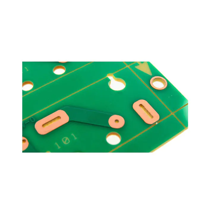
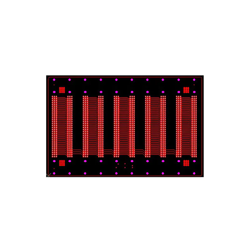
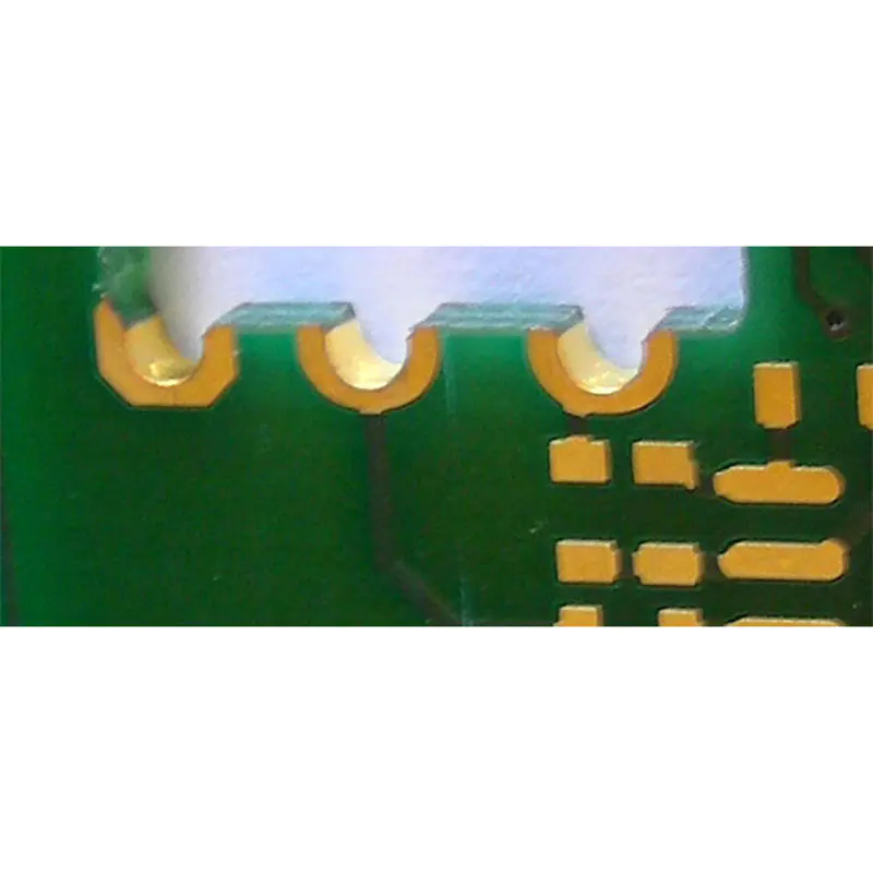

Blind Vias

Blind via is a copper plated hole that connects only one outer layer to one or more inner layers, it never goes all the way through a circuit board but only visible on one side of circuit boards. The blind via can be laser or mechanically drilled based on the detailed via hole size and layer stackup.
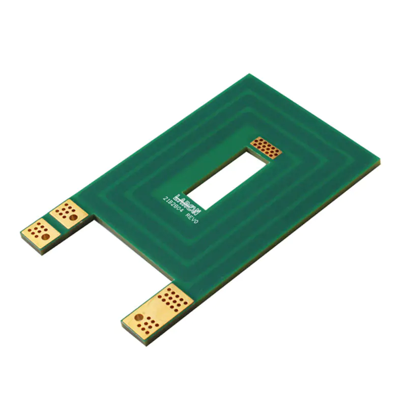
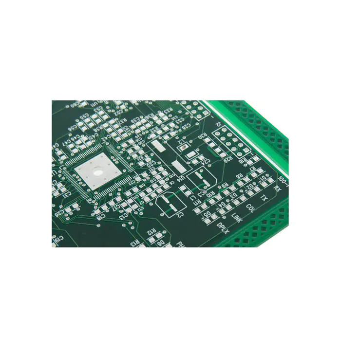

Buried Vias

Buried Via is a copper plated hole that connects two or more inner layers without contacting the outer layers, as the name suggests, it’s buried inside, so it’s not visible from the outer layer of PCB. Buried via has no impact to any trace or surface mount component on the top or bottom layers, trace or SMD pad can be placed directly over the buried via.

A-TECH CIRCUITS has capacity to build both of blind via and buried via with different demands, We’ll use laser drill for the blind vias with size smaller than 150um and use mechanical drill for the blind via size larger than 150um, the technology of blind via we can achieve include via in pad, stacked via and staggered via. The minimum size of buried via normally need to be 150um and they’ll be plugged with resin to avoid prepreg flow into buried via which might affect the connection with adjacent layers.


Company Features
1. Manufacturing facilities of A-TECH CIRCUITS Co., Ltd. are located worldwide. We have cultivated an in-house R&D team. They are responsible for the development of new innovative products and corporate with some famous laboratories in China.
2. Our factory is equipped with first-class production, testing, and research facilities. All these facilities are essential because they provide a solid foundation for reliable monthly product outputs.
3. Our R&D department is led by senior experts. These experts continuously develop new products based on market trends and introduce advanced development equipment. They are engaged in pursuing high-quality products to meet the needs of domestic and foreign markets. Keeping moving on and never setting back are important factors to success for A-TECH CIRCUITS Co., Ltd.. Contact!
Product Message

Loading verification code...

Please complete verification first

Chat Online 编辑模式下无法使用
Chat Online inputting...
Please hold on and we will get back to you soon