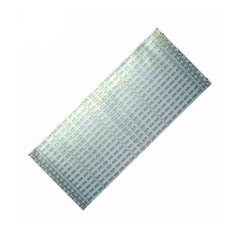
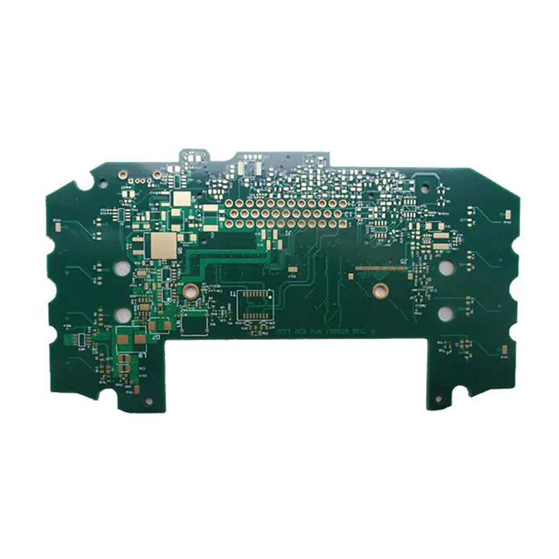
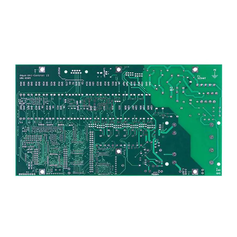
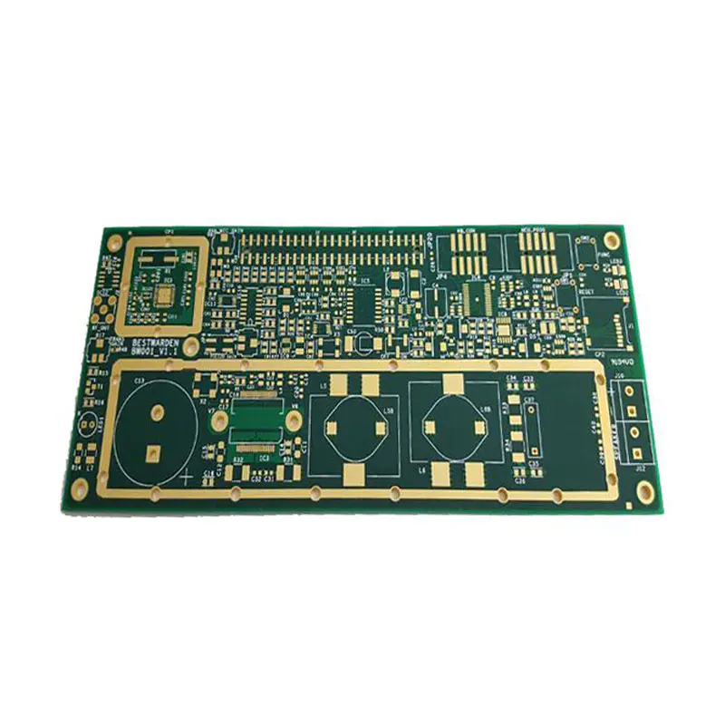
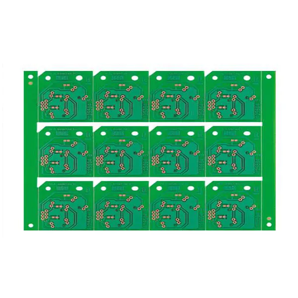
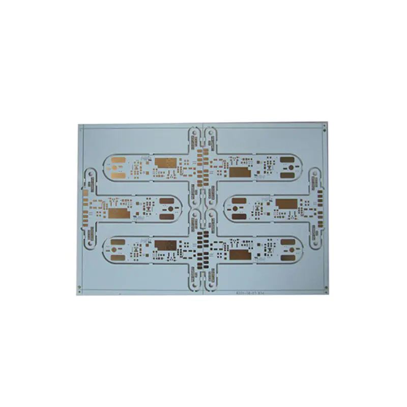
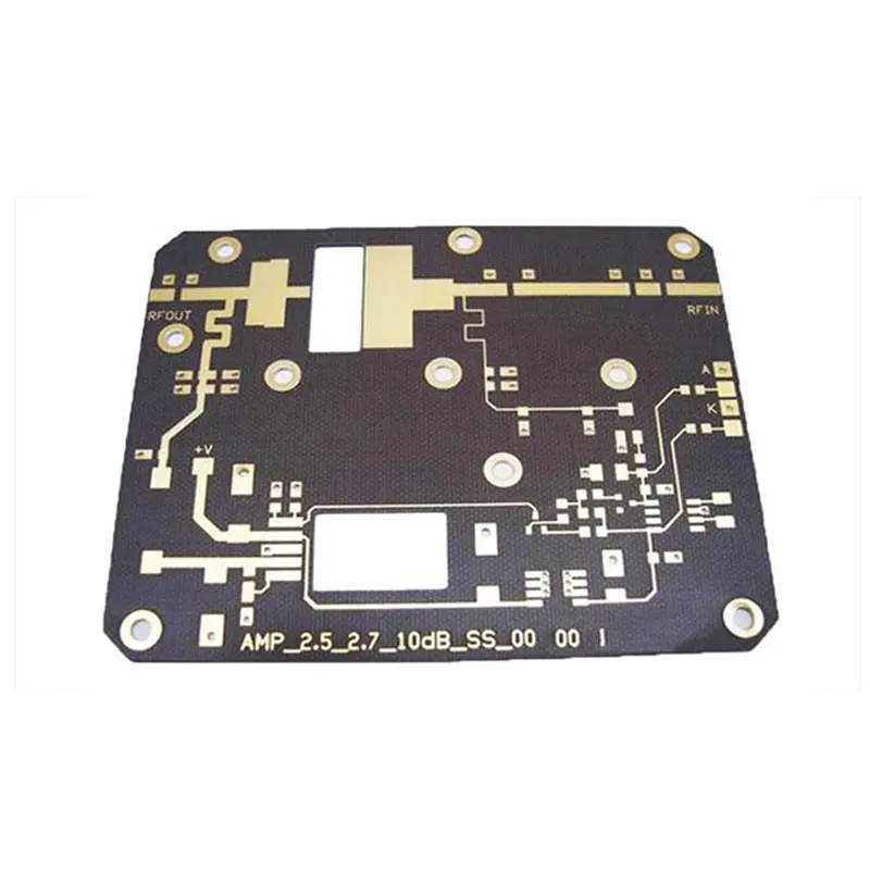
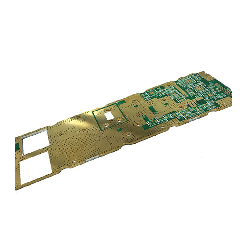
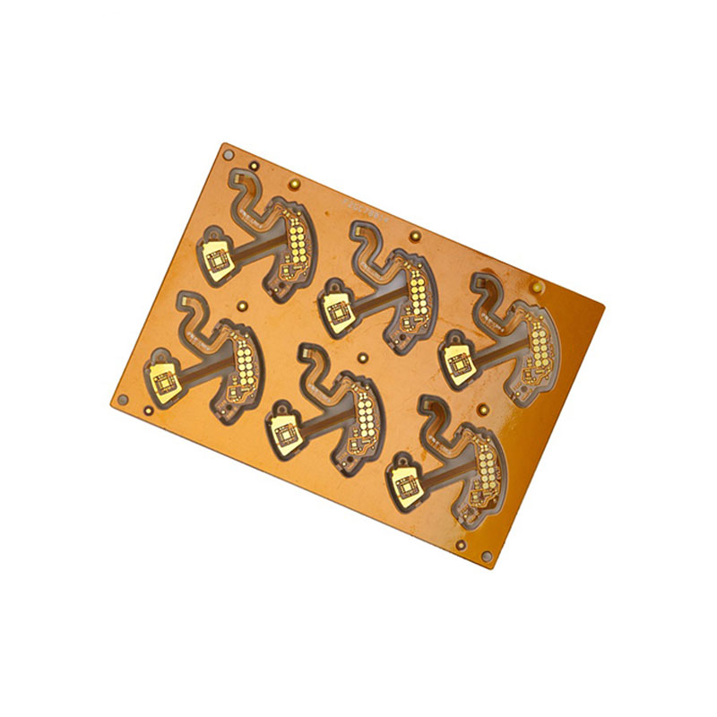
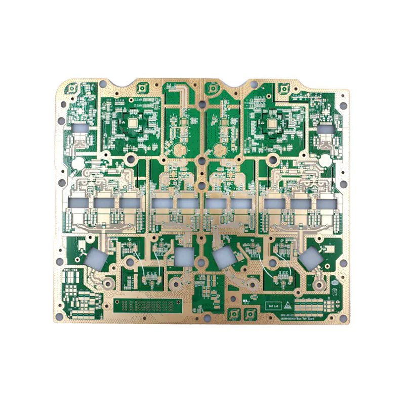
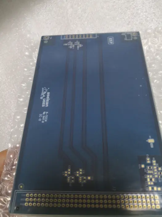
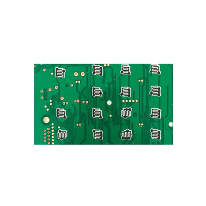
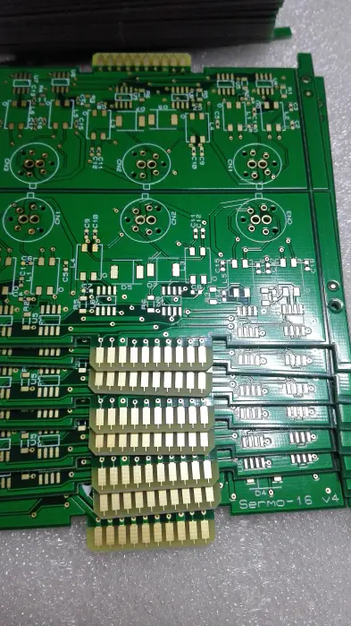
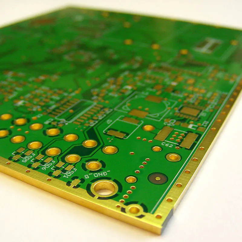
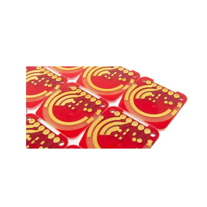
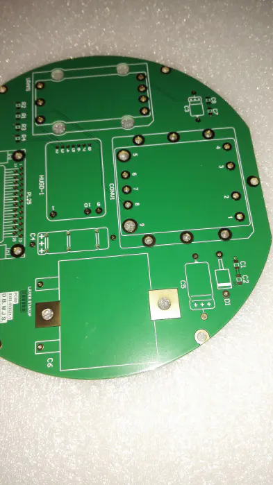
Related Products

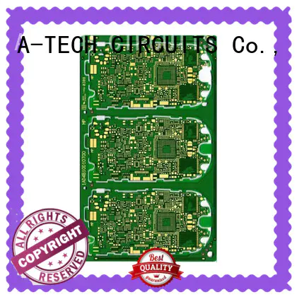

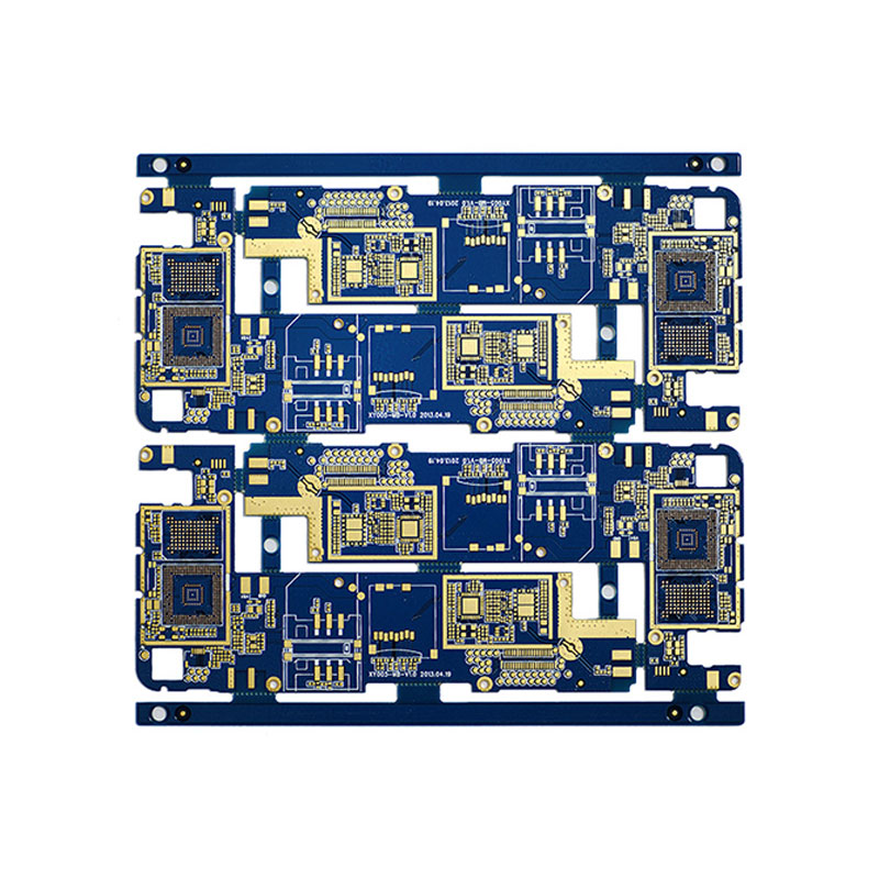
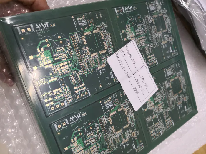
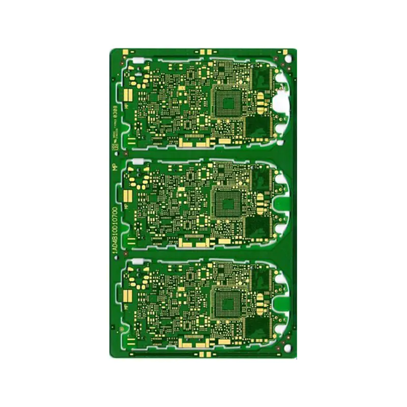
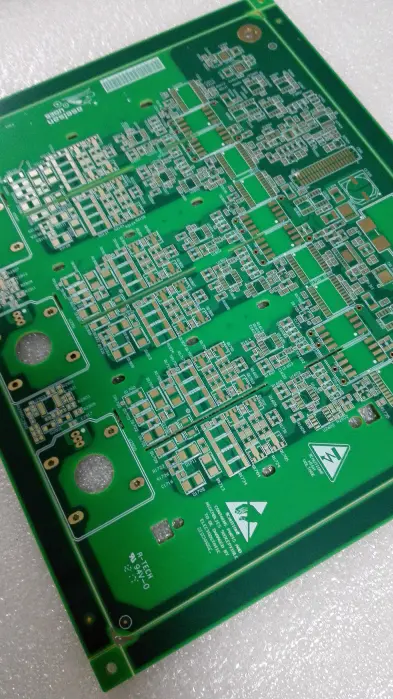
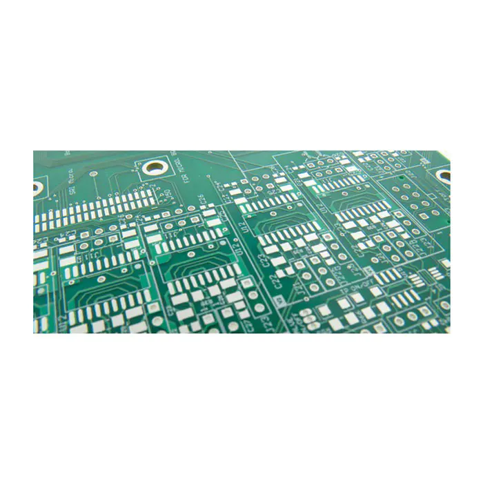
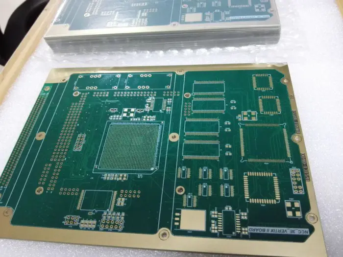
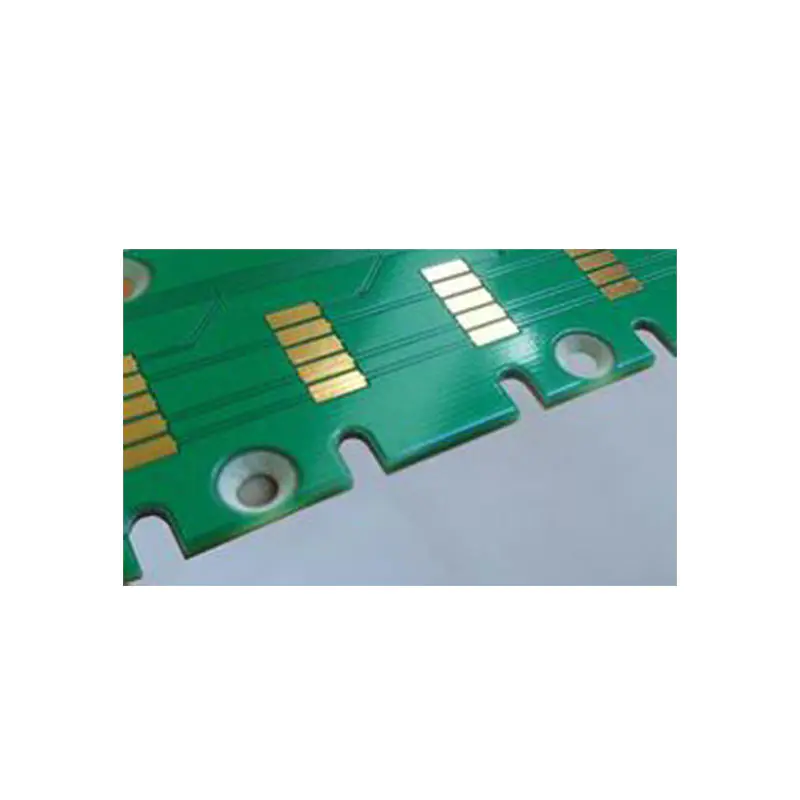
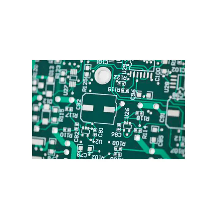
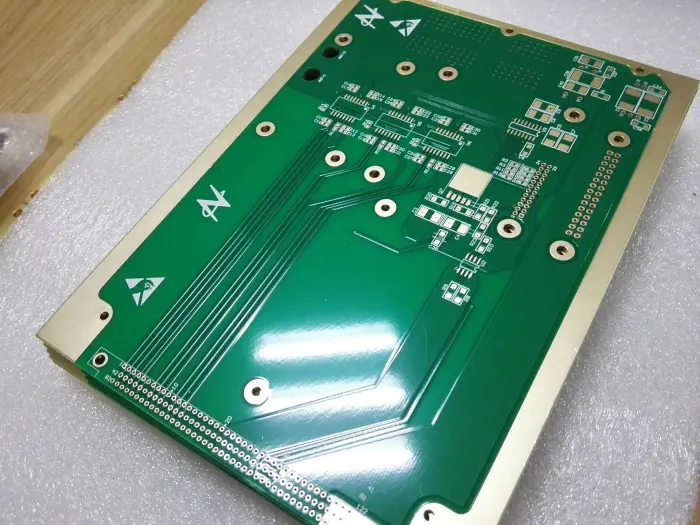
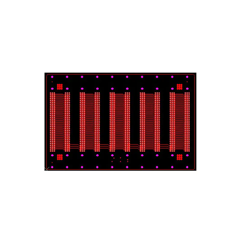
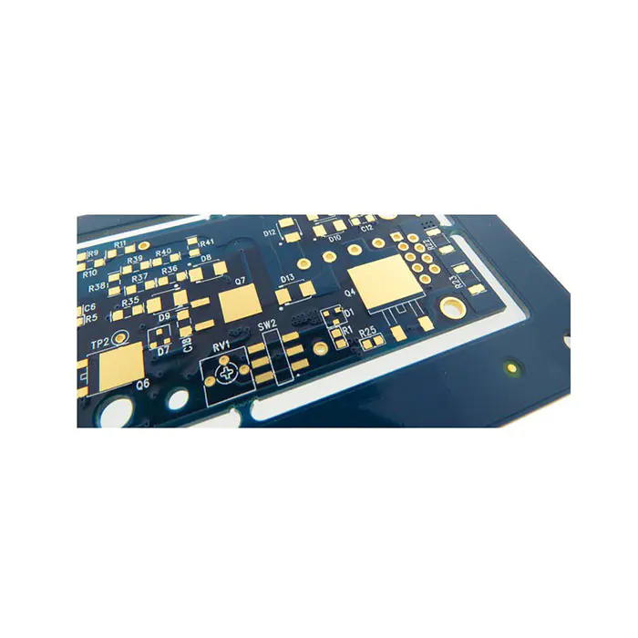
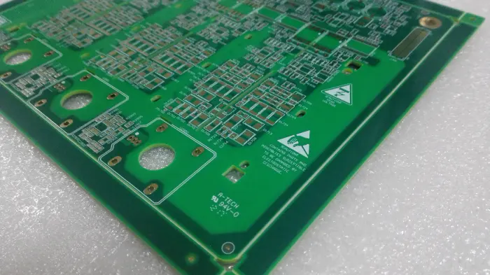
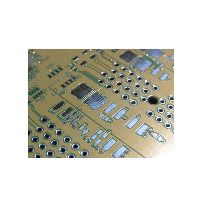
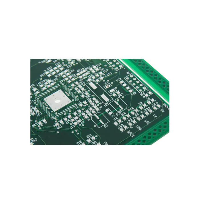
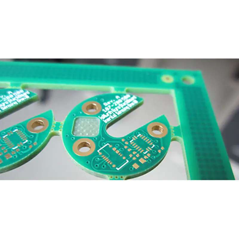
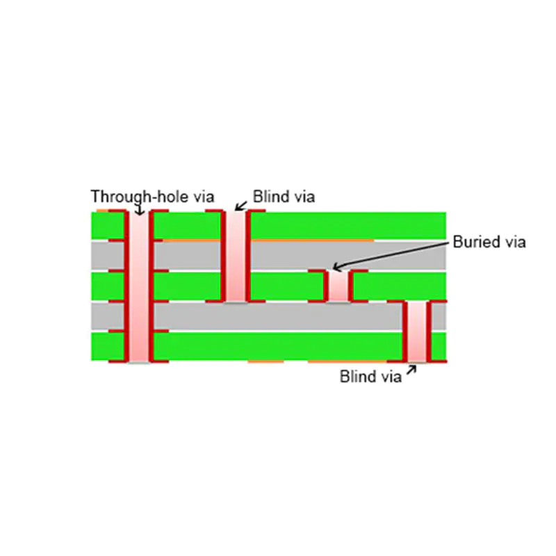
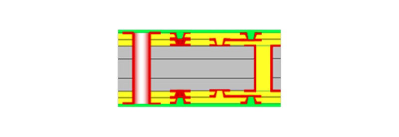
HDI PCB, the full name is High Density Interconnect PCB, it requires much higher wiring density with finer trace and spacing, smaller vias and higher connection pad density. Blind and buried vias’ design is one of their marked feature. HDI PCB are widely used for Cell phone, tablet computer, digital camera, GPS, LCD module and other different area.
The benefits of HDI PCB
● Reduce the cost
● Better reliability
● Increase the wiring density
● Increase design efficiency
● Can improve the thermal properties
● In favor of the use of advanced packaging technology
● Has better electrical performance and signal correctness
● Can improve the radio frequency interference, electromagnetic interference and electrostatic discharge
A-TECH CIRCUITS provides HDI PCB manufacturing services to worldwide customers in the high end automotive industry, medical electronic device industry, mobile, computing and defense industry.
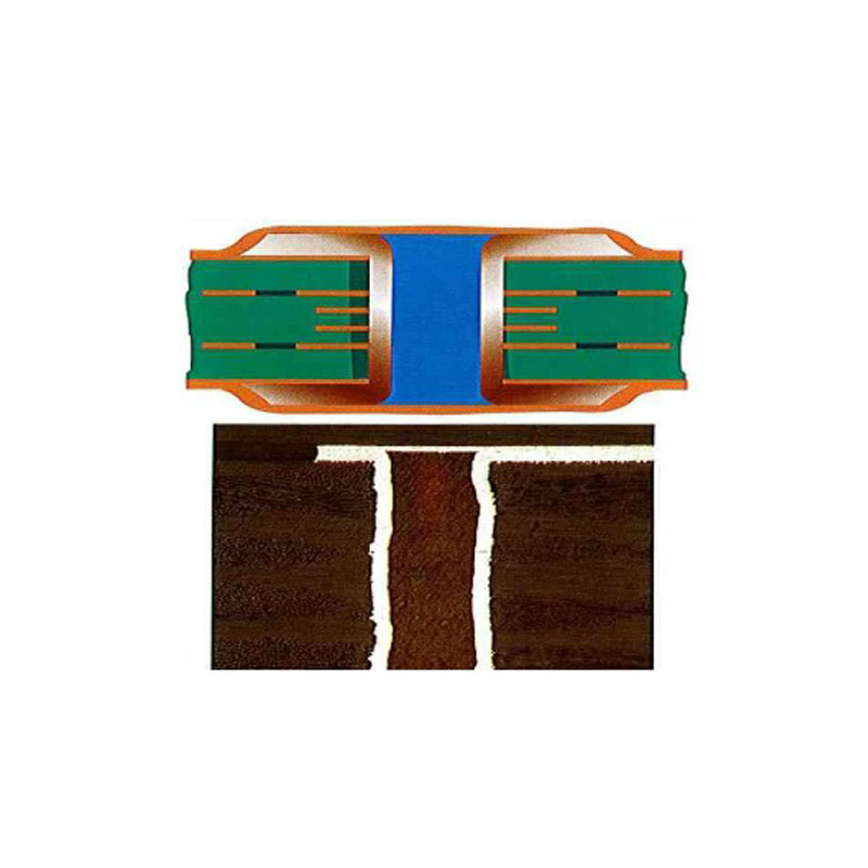
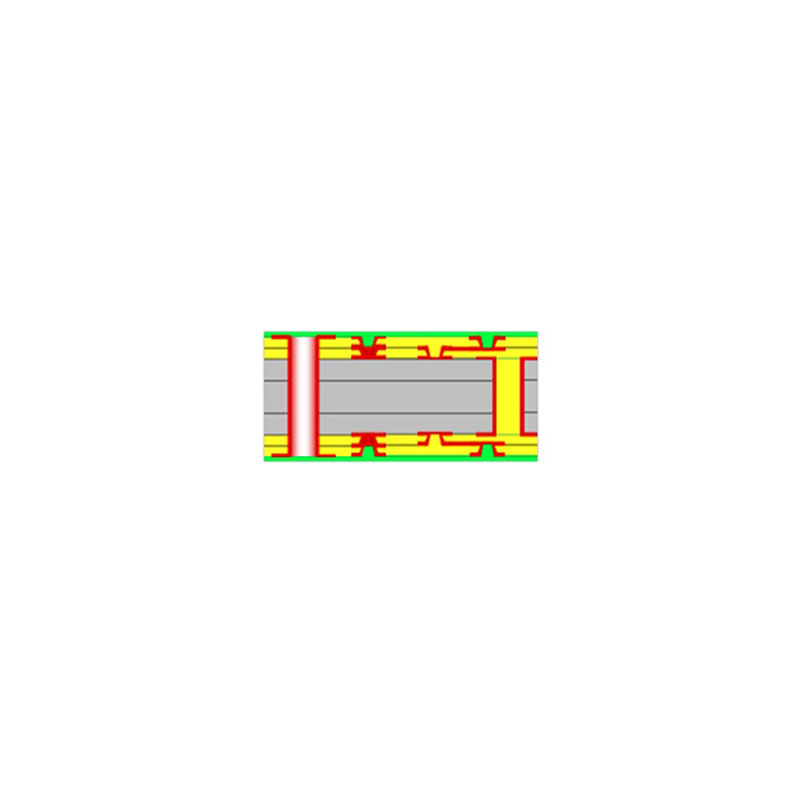
Currently the advanced HDI technology we used include: "Direct Laser Drill"(DLD) is drilling of copper layer by direct CO2 laser irradiation, compare to additional laser drilling with conformal mask, the copper direct laser drilling is capable of providing higher accuracy, better hole quality and better efficiency for HDI projects. "Copper Filled" for special stack microvia, "Laser Direct Imaging"(LDI) is specifically designed for fine line technology, to eliminate dimensional stability problem of artwork caused by environmental and material issues.
| General Specification for HDI PCB in A-TECH | |
| Layer Count | 4-20Layers |
| Type of stack up | 1+N+1, 2+N+2, 3+N+3 |
| Material Available | FR4, High Tg FR4, Halogen Free FR4 |
| Board thickness | 0.4-3.2mm |
| Finished copper thickness | 1-6oz |
| Finished copper thickness | 1/3oz – 2oz |
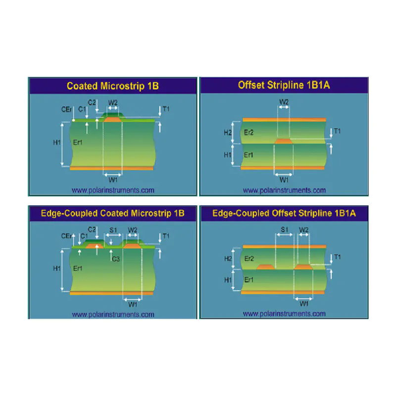
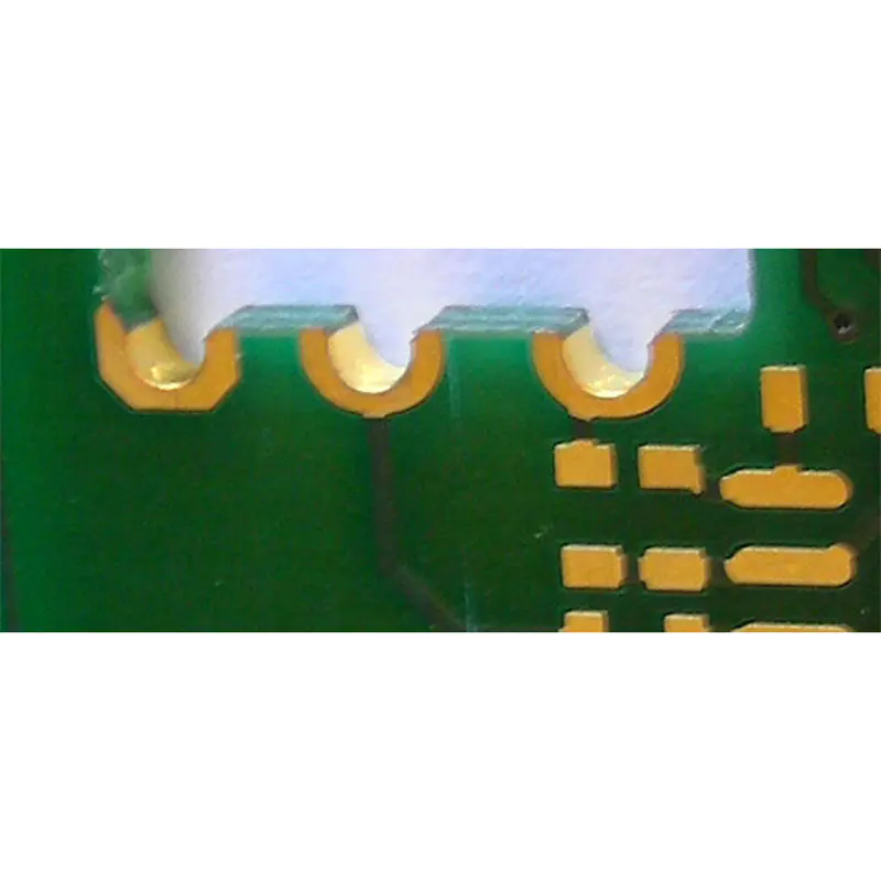
| Min trace width/spacing | 3/3mil |
| Min through hole | 0.2mm |
| Min blind via | 0.1mm |
| Types of blind via | Stack microvia, Stagger microvia |
| Surface treatment | Immersion Gold, Selective ENIG + OSP(BGA area) |
General inquiries & Customer Service
Tel: 86-755-2335 9039 | Fax: 86-755-3318 0939
E-Mail: Enquiry@atechcircuit.com
Skype: atechcircuits

Headquarters: 602, Building B3, Zhimei Huizhi Industrial Park, Fuyong Street, Bao'an District, Shenzhen City, China
Copyright © 2025 A-TECH CIRCUITS Co., Ltd. | All Rights Reserved
Hello, please leave your name and email here before chat online so that we won't miss your message and contact you smoothly.