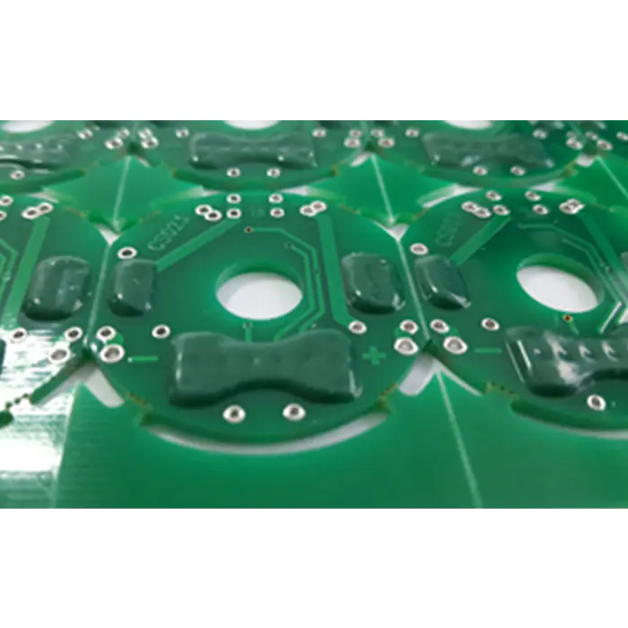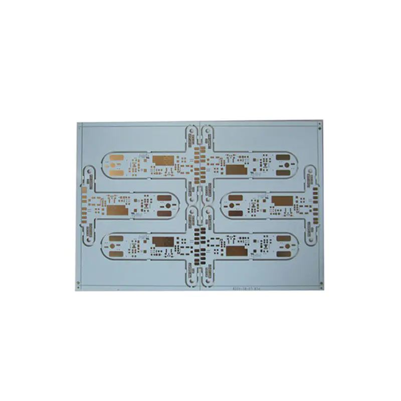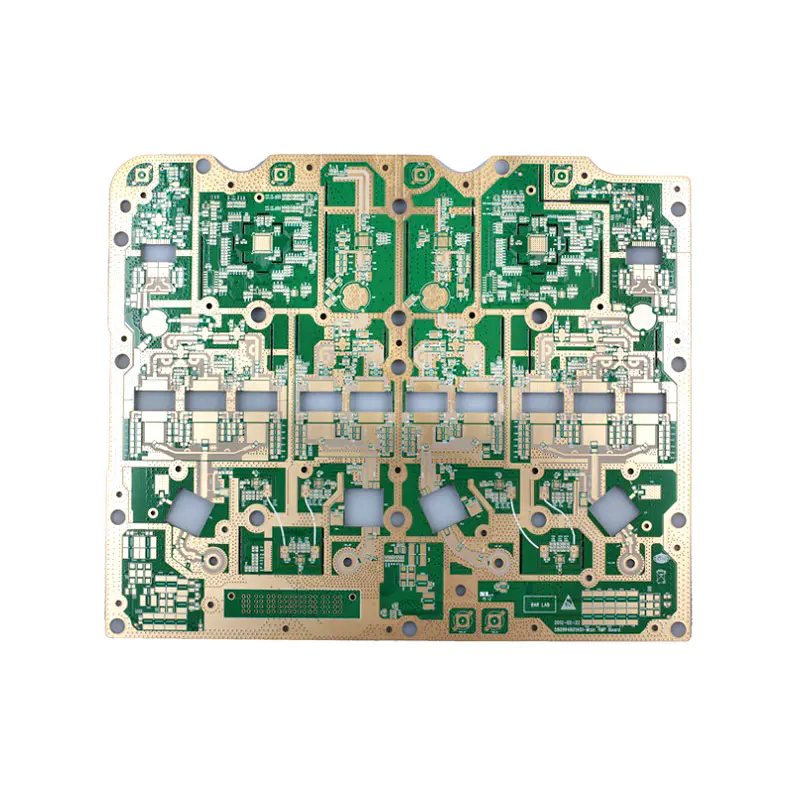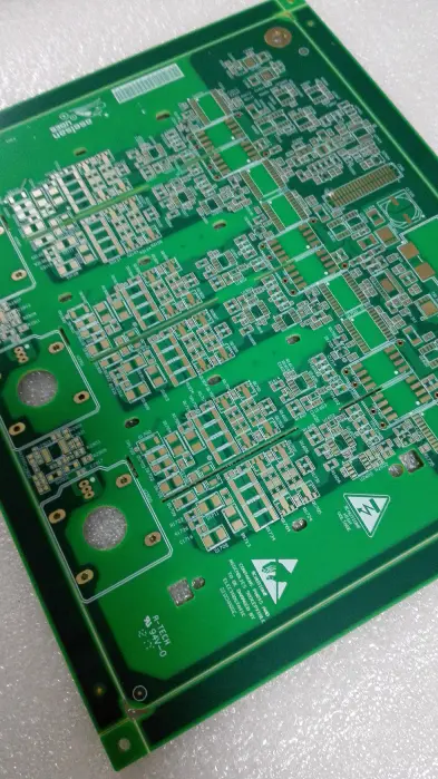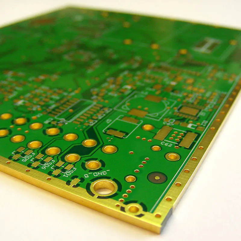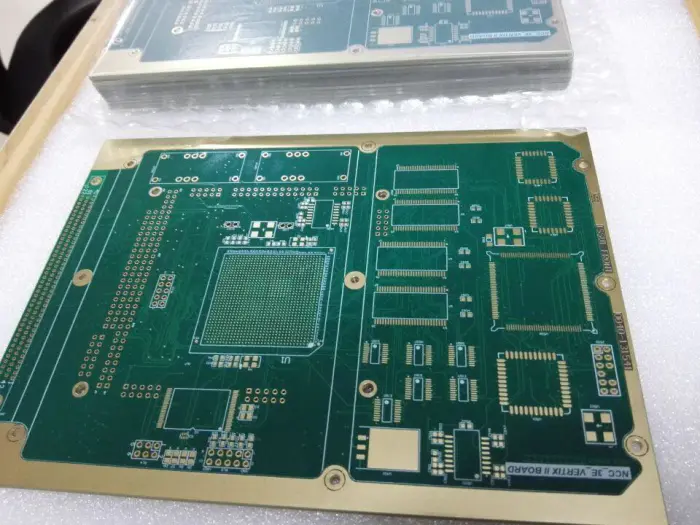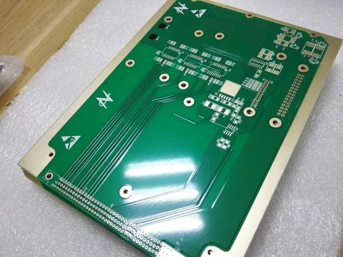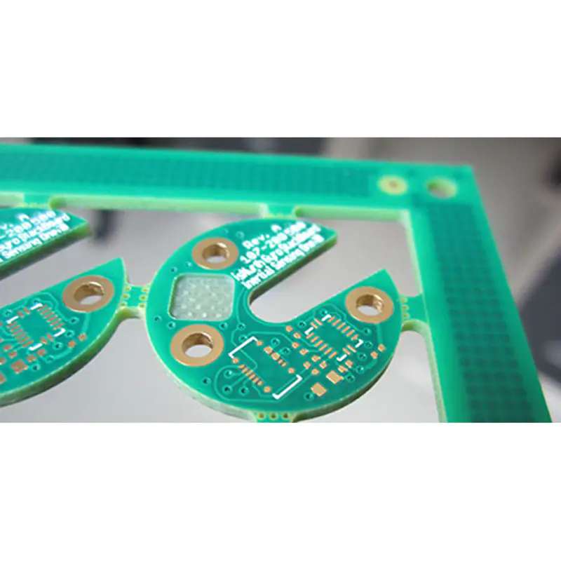
Double-sided PCB
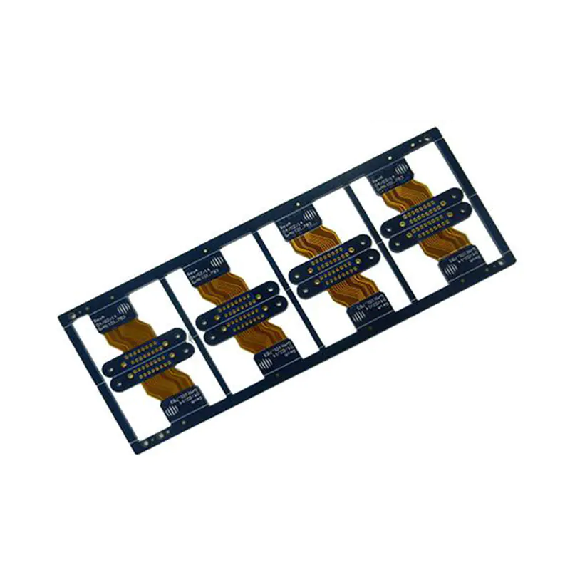
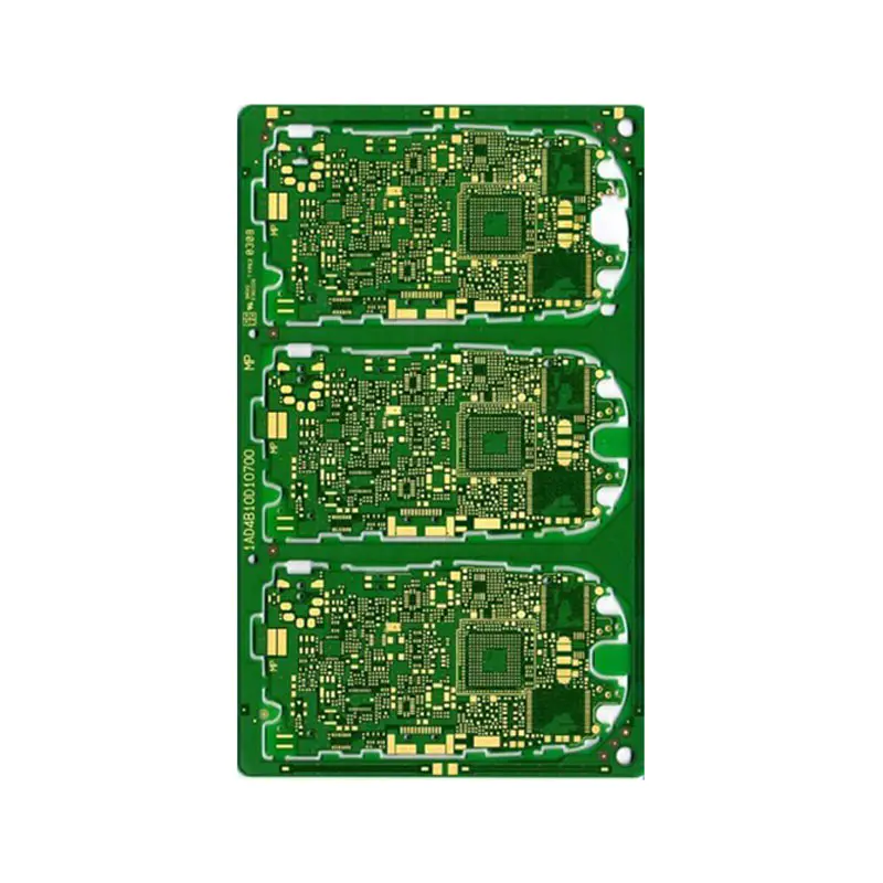
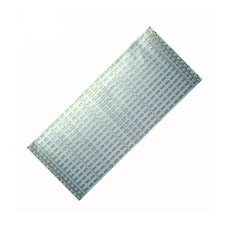
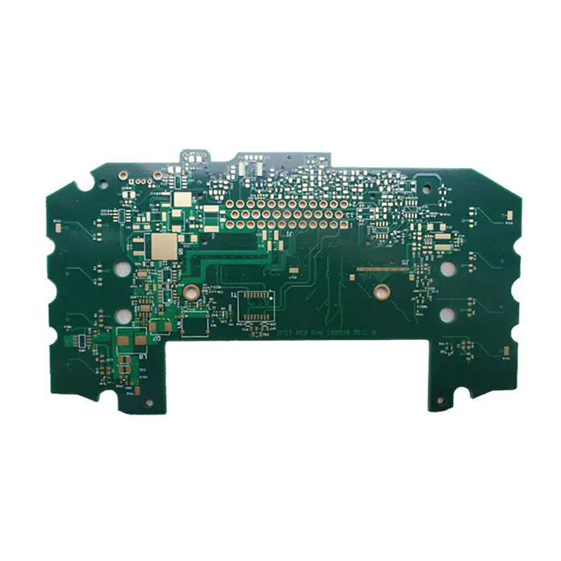
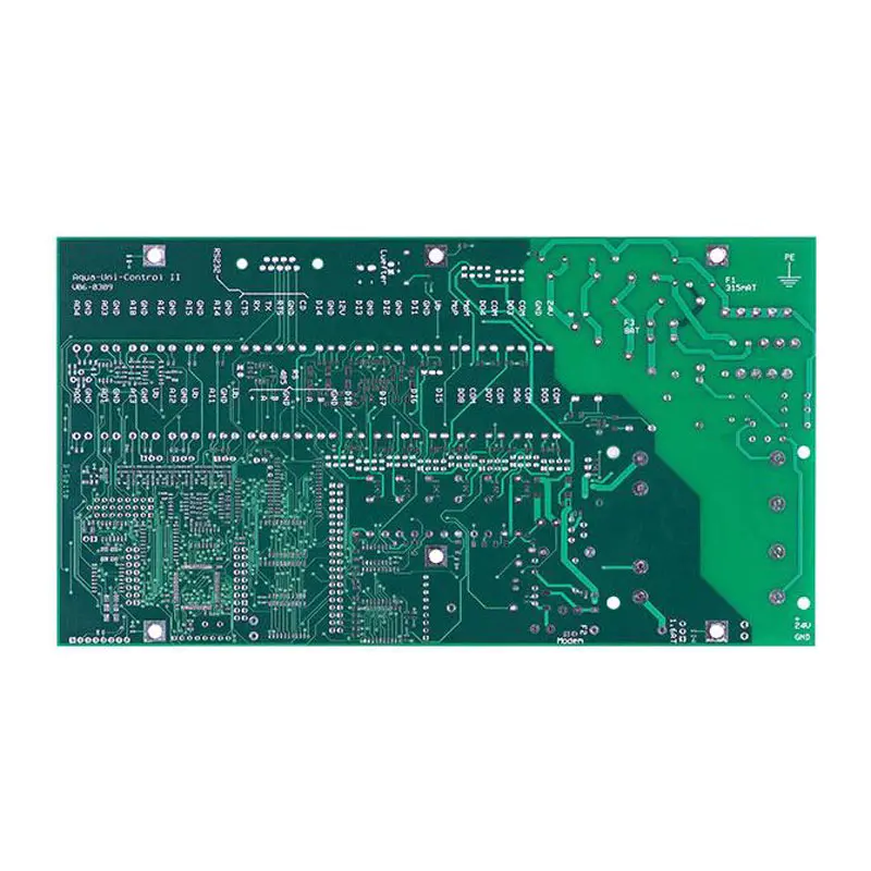
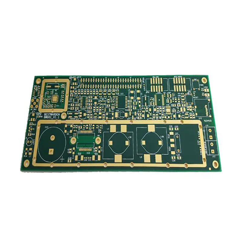
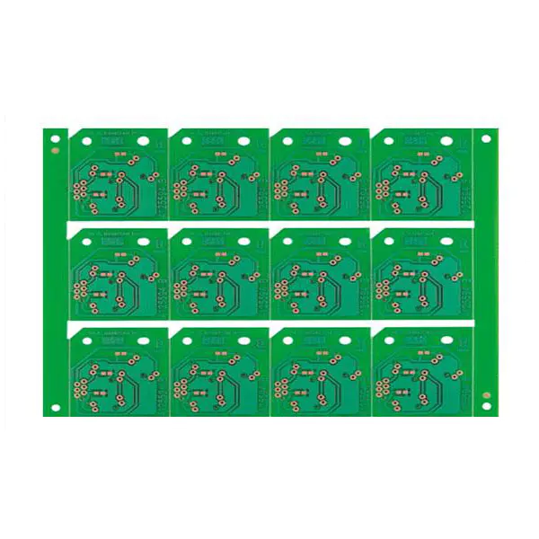
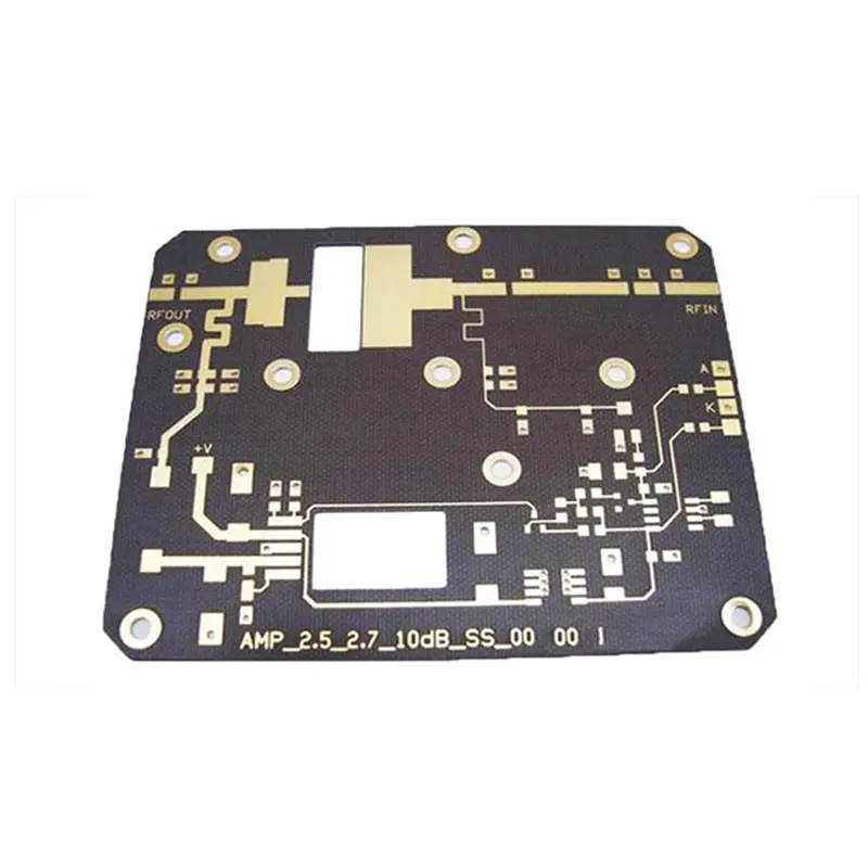
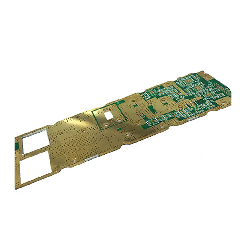
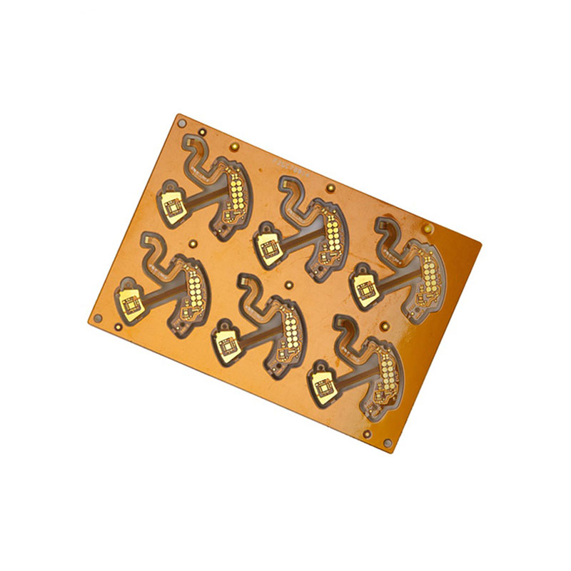
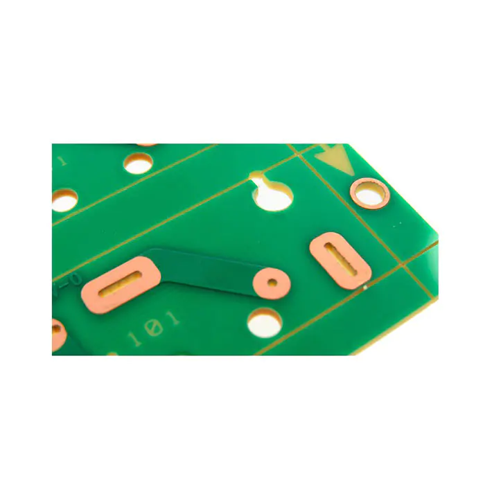
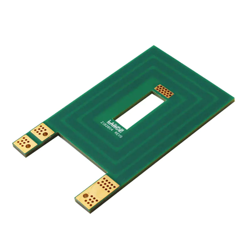
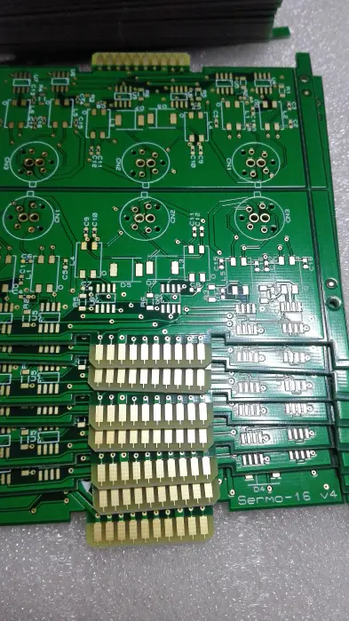
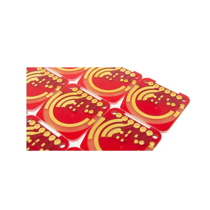
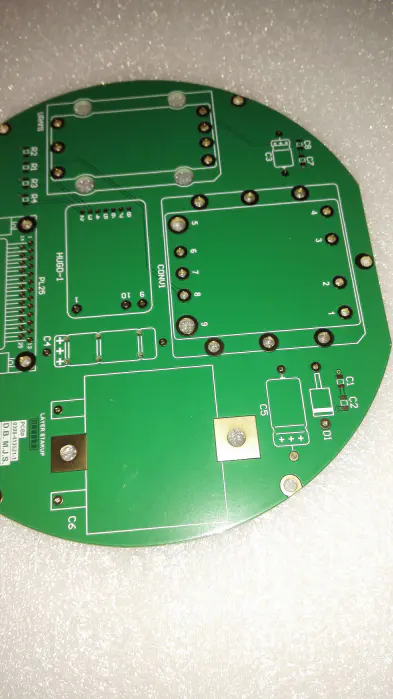
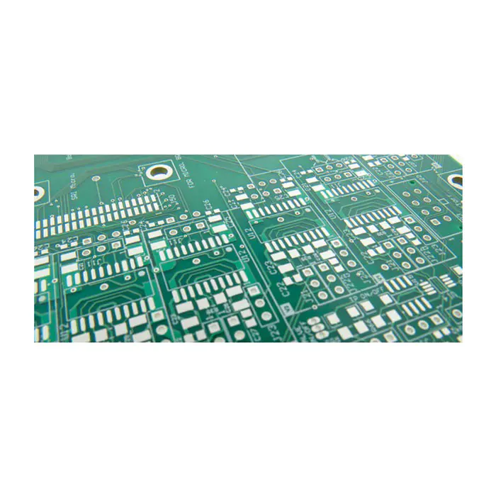
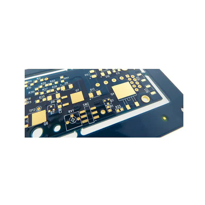
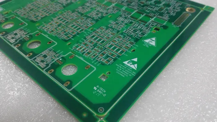
Related Products


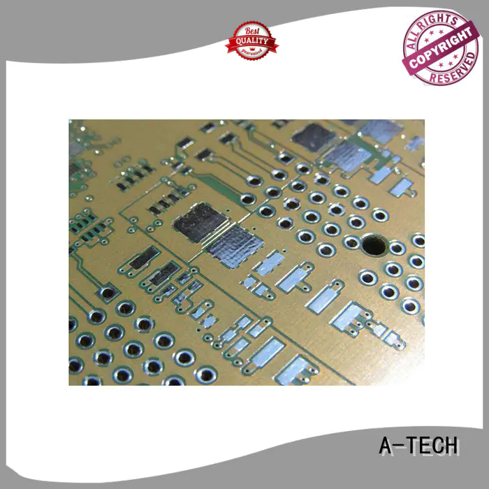
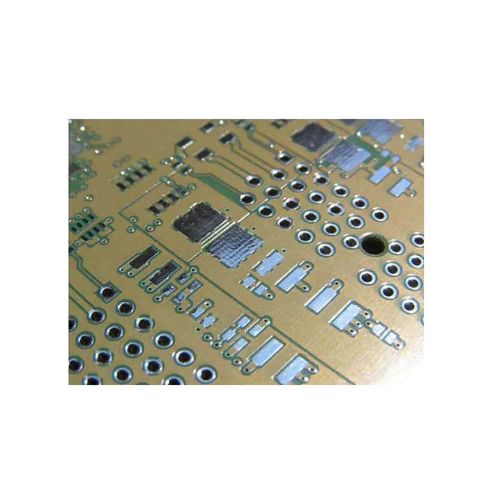
HAL(Lead Free), the full name is Hot Air leveling with Lead Free. Compared with HASL, the main difference for HAL(Lead Free) is the element of material which do not contain Lead(Pb), so it’s RoHS Compliant and it’s much more popular and widely used in PCB manufacturing.
HAL(Lead Free) requires higher run temperatures for lead free solder and longer contact time, the production cost for HAL(Lead Free) is slightly higher than HASL(Tin/Lead).
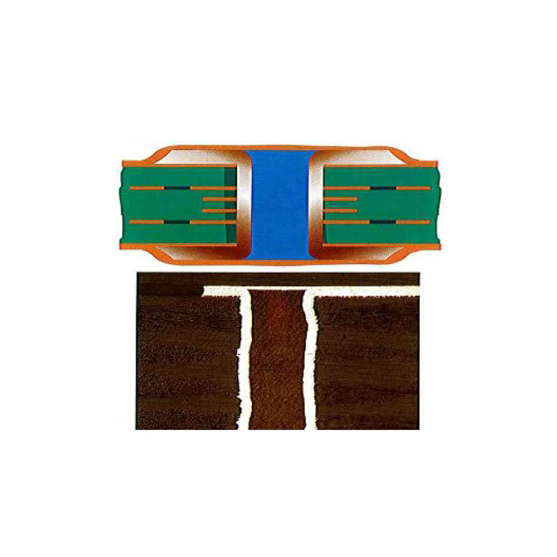
The manufacturing process of HAL(Lead Free) is similar to HASL(Tin/Lead), the circuit boards will be submersed in molten solder(Lead Free). This solder will cover all the exposed copper surfaces. Upon retraction from the solder, high pressure hot air is blown over the surface through air knives, this levels the solder deposit and removes the excess solder from the surface of printed circuit boards.
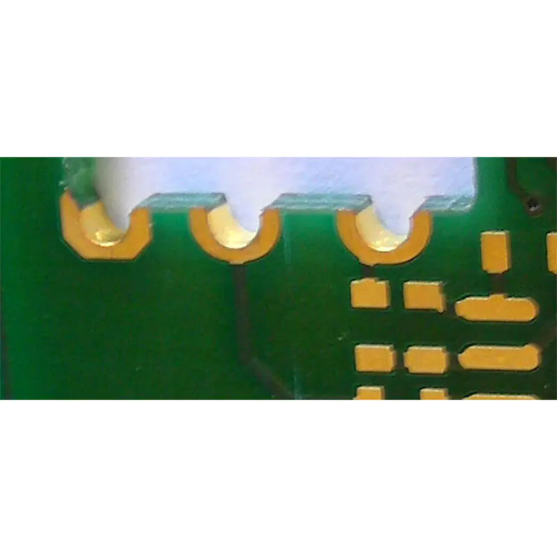
The typical thickness of HAL(Lead Free) is 1-40um and the shelf life is 12 months.
The advantages of HAL(Lead Free) surface finish
● Good solderability / wettability
● RoHS Compliant
● Good reflow properties
● Large processing window is allowed
● Multiple thermal excursions
● Can be widely used
The disadvantages of HAL(Lead Free) surface finish
● Uneven surface
● Not suitable for PCBs with fine pitch
● Thermal shock
● Solder bridge
● Plugged or Reduced plated through holes
A-TECH have HAL(Lead Free) surface finish in house, It’s basically the highest proportion of finish used for circuit boards without fine pitch or high density layout. We don’t have any additional cost for HAL(Lead Free) surface finish.
General inquiries & Customer Service
Tel: 86-755-2335 9039 | Fax: 86-755-3318 0939
E-Mail: Enquiry@atechcircuit.com
Skype: atechcircuits

Headquarters: 602, Building B3, Zhimei Huizhi Industrial Park, Fuyong Street, Bao'an District, Shenzhen City, China
Copyright © 2025 A-TECH CIRCUITS Co., Ltd. | All Rights Reserved
Hello, please leave your name and email here before chat online so that we won't miss your message and contact you smoothly.