
The small holes on the PCB are vias, used to connect electrical signals from one layer to another.
The holes on the pcb board can be divided into three types, screw holes, conductive holes, plug-in holes.
The screw holes are used for fixing.
Conductive holes (also called over-electric holes) are used to conduct electricity just like wires.
The plug-in hole is of course used to insert various parts, such as diodes, transistors, capacitors, inductors and so on.
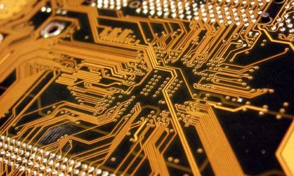
PCB is divided into single-sided PCB board, double-sided PCB board, and multi-layer PCB board, and the board with more than two sides is connected with the conductive hole from one side to the other side.
1. Some net lines must be perforated on two layers
2. Two layers of large-area ground GND and many holes are drilled to reduce noise and buffer the circuit board deformation.
Those vias are used to connect electrical signals from one layer to another layer.
In addition, the small hole is usually a via, not only for conduction, many reasons can reduce the parasitic capacitance caused by copper and platinum on both sides, which means to eliminate the effect of parasitic capacitance, and the other is to increase the conductivity .. ....
The holes in the PCB are divided into PTH and NPTH holes, that is, through holes and non-through holes. The through holes play a role of conduction between the layers after the copper plate is powered, that is, the first layer line and the second layer line Conductive and non-conductive holes are divided into positioning holes and plug-in holes, which are used to insert components into SMT placement.
General inquiries & Customer Service
Tel: 86-755-2335 9039 | Fax: 86-755-3318 0939
E-Mail: Enquiry@atechcircuit.com
Skype: atechcircuits

Headquarters: 602, Building B3, Zhimei Huizhi Industrial Park, Fuyong Street, Bao'an District, Shenzhen City, China
Copyright © 2025 A-TECH CIRCUITS Co., Ltd. | All Rights Reserved
Hello, please leave your name and email here before chat online so that we won't miss your message and contact you smoothly.


