
In the process of PCB manufacturing, in order to ensure the production quality of PCB boards, PCB manufacturers usually use a variety of detection methods for different PCB defects in the production process.
1. Manual visual inspection of PCB board
Using a magnifying glass or a calibrated microscope, the visual inspection of the operator is used to determine whether the circuit board is unqualified, and to determine when correction operations are required. However, due to the increased production of PCBs and the reduction in the spacing of wires on the PCB and the volume of components, this method has become less and less feasible.
2. Online test of PCB board
Through the inspection of electrical performance to find manufacturing defects and test analog, digital and mixed signal components to ensure that they meet the specifications, there are several test methods such as needle bed testers and flying probe testers.
3. PCB board function test
The functional system test is to use special test equipment at the middle and end of the production line to comprehensively test the functional modules of the circuit board to confirm the quality of the circuit board. Functional testing can be said to be the earliest automatic testing principle. It is based on a specific board or a specific unit and can be completed with various devices. There are types of final product testing, the latest solid model and stacked testing. Functional testing usually does not provide deep-level data such as foot-level and component-level diagnostics for process improvement, and requires special equipment and a specially designed test process. Writing functional test procedures is complicated, so it is not suitable for most circuit board production lines.
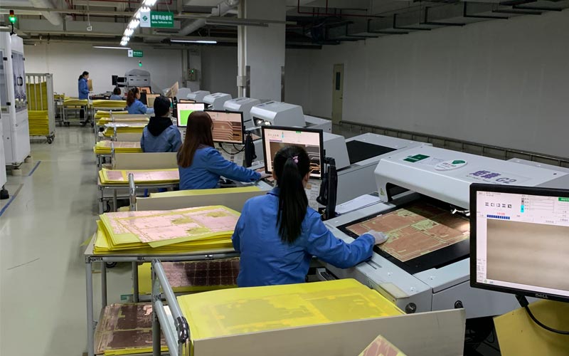
4. Automatic optical Inspection(AOI)
Also known as automatic visual inspection, it is based on the principle of optics and uses a variety of technologies such as image analysis, computer and automatic control to detect and process defects encountered in the production of circuit boards. It is a relatively new method of confirming manufacturing defects. AOI is usually used before and after reflow and before electrical testing to improve the pass rate in the electrical processing or functional testing phase. At this time, the cost of correcting defects is much lower than the cost of conducting after the final test, often reaching a dozen times.
5. Automatic X-ray inspection
Using the difference in the absorption rate of X-rays by different substances, see through the parts to be detected and find defects. It is mainly used to detect defects such as ultra-fine pitch and ultra-high-density circuit boards and bridging, chip dropping, and misalignment during the assembly process. It can also use its tomography technology to detect internal defects in IC chips. It is currently the only way to test the soldering quality of the ball grid array and the blocked solder balls.
6. Laser detection system
This is the latest development in PCB testing technology. Use the laser beam to scan the printed board, collect all measurement data, and compare the actual measurement value with the preset qualified limit value. This technology has been confirmed on the light board, and is being considered for assembly board testing. The speed is sufficient for mass production lines.
7. Size detection
Use the 2-D image measuring instrument to measure the size of the hole position, length, width and position. Since PCBs are small, thin and soft products, contact measurement can easily deform and cause inaccurate measurements. The second-dimensional image measuring instrument has become the best high-precision dimension measuring instrument.
General inquiries & Customer Service
Tel: 86-755-2335 9039 | Fax: 86-755-3318 0939
E-Mail: Enquiry@atechcircuit.com
Skype: atechcircuits

Headquarters: 602, Building B3, Zhimei Huizhi Industrial Park, Fuyong Street, Bao'an District, Shenzhen City, China
Copyright © 2025 A-TECH CIRCUITS Co., Ltd. | All Rights Reserved
Hello, please leave your name and email here before chat online so that we won't miss your message and contact you smoothly.


