
The uneven copper surface area on the circuit board will worsen the board bending and board warpage
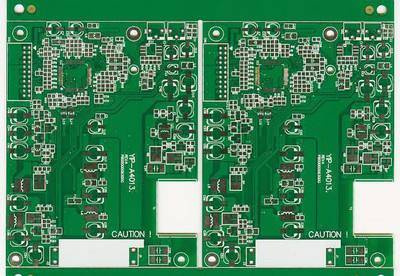
Generally, a large area of copper foil is designed on the circuit board for grounding. Sometimes, a large area of copper foil is also designed on the Vcc layer. When these large area copper foils cannot be evenly distributed on the same piece When it is on the circuit board, it will cause the problem of uneven heat absorption and heat dissipation speed. Of course, the circuit board will also expand and contract with heat. If the upper limit of the Tg value has been reached, the circuit board will begin to soften, causing permanent deformation.
The connection points (vias) of the various layers on the circuit board will limit the board's expansion and contraction.
Most circuit boards are multilayer printed circuit boards, and there will be rivet-like connection points (vias) between the layers. The connection points are divided into through holes, blind holes, and buried holes. Where there are connection points, multiple layers will be restricted. The effect of circuit board board expansion and contraction will also indirectly cause circuit board board bending and board.
General inquiries & Customer Service
Tel: 86-755-2335 9039 | Fax: 86-755-3318 0939
E-Mail: Enquiry@atechcircuit.com
Skype: atechcircuits

Headquarters: 602, Building B3, Zhimei Huizhi Industrial Park, Fuyong Street, Bao'an District, Shenzhen City, China
Copyright © 2025 A-TECH CIRCUITS Co., Ltd. | All Rights Reserved
Hello, please leave your name and email here before chat online so that we won't miss your message and contact you smoothly.


