
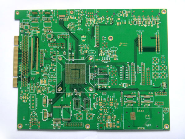
HDI PCB is a type of printed circuit board, which is called high Density Interconnection PCB. High-density interconnection board At present, high-end electronic products are generally HDI products.
With the current development of portable product design in the direction of miniaturization and high density, the difficulty is becoming greater and greater, and higher requirements are placed on the PCB manufacturing process. Most of the current portable products use the design process of blind buried vias for BGA packages with a pitch below 0.65mm, so what is blind buried vias?
Blind vias (Blindvias): Blind vias are the type of vias that connect the inner traces of the PCB to the traces on the surface of the circuit board. This hole does not penetrate the entire board.
Buried vias: Buried vias are only via types that connect the traces between the inner layers, so they are not visible from the PCB surface.
Circuit boards with buried blind holes are not necessarily HDI circuit boards, but generally HDI boards have blind holes, and buried holes are not necessary. It depends on your circuit board products.
For example, The one step and two step in the 6-layer circuit board are for boards that require laser drilling, which refers to HDI PCB boards.
6-layer circuit board one step HDI board refers to blind holes: 1-2, 2-5, 5-6. That is, 1-2, 5-6 require laser drilling.
6-layer circuit board two step HDI board refers to blind holes: 1-2, 2-3, 3-4, 4-5, 5-6. 2 laser drillings are required.
General inquiries & Customer Service
Tel: 86-755-2335 9039 | Fax: 86-755-3318 0939
E-Mail: Enquiry@atechcircuit.com
Skype: atechcircuits

Headquarters: 602, Building B3, Zhimei Huizhi Industrial Park, Fuyong Street, Bao'an District, Shenzhen City, China
Copyright © 2025 A-TECH CIRCUITS Co., Ltd. | All Rights Reserved
Hello, please leave your name and email here before chat online so that we won't miss your message and contact you smoothly.


