
Classification of Fiducial Mark points in PCB design
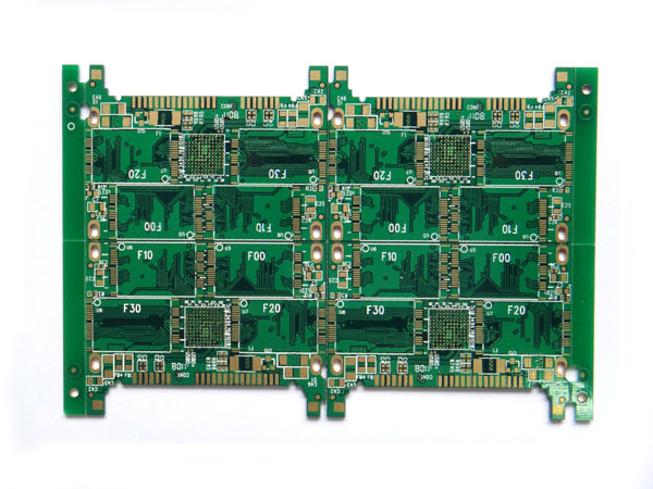
1) Mark points are used for optical positioning during solder paste stencil printing and component placement. According to the role of Mark points, it can be divided into puzzle Mark points, single board Mark points, local Mark points (also called device-level MARK points).
2) There should be at least three Mark points on the process edge of the panel and the single board that does not need to be panel-shaped, distributed in an L shape, and the diagonal Mark points are asymmetric about the center.
3) If there are mounted components on both sides, there should be Mark points on each side.
4) The PCB design needs to have as many Mark points as possible on the single board. If there is no position to place Mark points, Mark points may not be placed on the board.
5) For devices such as QFP with lead center distance ≤0.5 mm and BGA with center distance ≤0.8 mm, local Mark points should be set diagonally near the diagonal line passing through the center point of the component, so as to accurately position them.
6) If several SOP devices are relatively close (≤100mm) to form an array, they can be regarded as a whole, and two local Mark points are designed at their diagonal positions.
PCB design instructions and size requirements:
1) The shape of the Mark point is a solid circle with a diameter of 1mm, the material is copper, the surface is tinned, pay attention to the flatness, the edge is smooth and neat, and the color is obviously different from the surrounding background color; , For the puzzle and veneer diameter is 3mm, for the local Mark point diameter is 1mm.
2) The Mark point on the board should be no less than 5mm from the center of the board; the Mark point on the craft side should be no less than 3mm from the center of the board.
3) In order to ensure the printing and recognition effects, there should be no pads, vias, dots, traces, and silk-screen markings within the range of Mark points, which cannot be cut by the V-CUT slot and cannot be recognized by the machine.
4) In order to increase the contrast between the Mark point and the substrate, copper foil can be laid under the Mark point. The inner background of the Mark points on the same board should be the same, that is, whether there is copper foil under the Mark points should be consistent.
5) Mark points for single board and panel should be designed as components, and local Mark points should be designed as part of component packaging. It is convenient to assign accurate coordinate values for positioning.
General inquiries & Customer Service
Tel: 86-755-2335 9039 | Fax: 86-755-3318 0939
E-Mail: Enquiry@atechcircuit.com
Skype: atechcircuits

Headquarters: 602, Building B3, Zhimei Huizhi Industrial Park, Fuyong Street, Bao'an District, Shenzhen City, China
Copyright © 2025 A-TECH CIRCUITS Co., Ltd. | All Rights Reserved
Hello, please leave your name and email here before chat online so that we won't miss your message and contact you smoothly.


