
Common drilling holes for PCBs in circuit board factories: through holes, blind holes, and buried holes. The meaning and characteristics of these three holes as following:
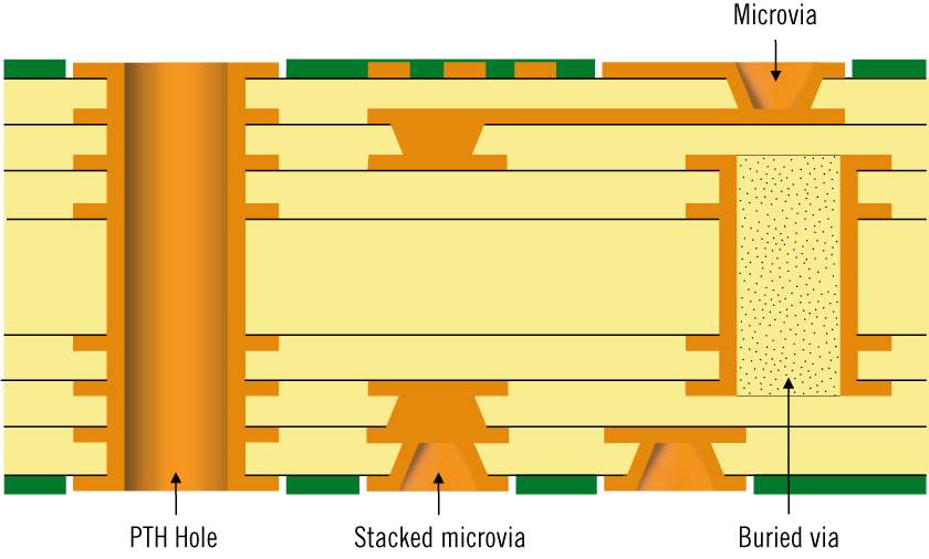
1. Via hole (VIA), this is a common hole used for conducting or connecting copper foil lines between conductive patterns in different layers of the circuit board, but it cannot be inserted into component lead legs or other reinforcing materials plated copper holes.
Because the PCB is formed by stacking and stacking many copper foil layers, an insulation layer is laid between each copper foil layer, so that the copper foil layers cannot communicate with each other, and the signal link depends on the via hole (Via), so it has the title of Chinese vias. The characteristics are: In order to meet the needs of customers, the via holes of the circuit board must be plugged. In this way, in the traditional aluminum plug hole process, the white board is used to complete the solder mask and plug hole of the circuit board surface, so that the production is stable. The quality is reliable and the application is more perfect. Vias are mainly used for the interconnection and conduction of circuits. With the rapid development of the electronics industry, higher requirements are also placed on the process and surface mount technology of printed circuit board production.
2. Blind hole: It is to connect the outermost circuit in the PCB to the adjacent inner layer with a plated hole. Because it cannot see the opposite side, it is called blind pass. At the same time, in order to increase the space utilization between PCB circuit layers, blind holes are applied. That is, a via hole to one surface of the printed circuit board.
Features: The blind holes are located on the top and bottom surfaces of the circuit board and have a certain depth. They are used for the connection of the surface layer circuit and the inner layer circuit below. The depth of the hole usually does not exceed a certain ratio (aperture). This production method requires special attention to the depth of the drill hole (Z axis) to be just right. If you don’t pay attention, it will cause difficulty in plating in the hole, so it is almost not used by the PCB factory. Drill holes first and then glue them together, but more precise positioning and alignment devices are needed.
3. Buried hole: It means the link between any circuit layers inside the PCB but does not lead to the outer layer, and also means a via hole that does not extend to the surface of the circuit board.
Features: In this process, it is not possible to use the method of drilling after bonding. Drilling must be performed at the individual circuit layer, the inner layer is first partially bonded, and then the plating process is performed before the final bonding can be completed, which is better than the original conduction. Holes and blind holes take more time, so the price is also the most expensive. This process is usually only used on high-density printed circuit boards to increase the usable space of other circuit layers.
General inquiries & Customer Service
Tel: 86-755-2335 9039 | Fax: 86-755-3318 0939
E-Mail: Enquiry@atechcircuit.com
Skype: atechcircuits

Headquarters: 602, Building B3, Zhimei Huizhi Industrial Park, Fuyong Street, Bao'an District, Shenzhen City, China
Copyright © 2025 A-TECH CIRCUITS Co., Ltd. | All Rights Reserved
Hello, please leave your name and email here before chat online so that we won't miss your message and contact you smoothly.


