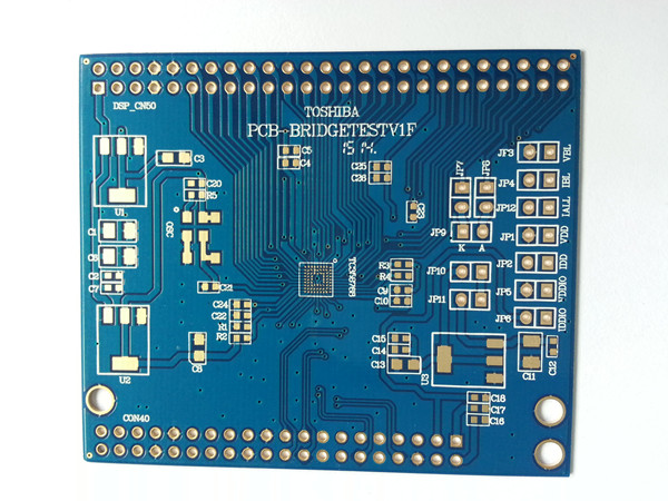
Compared with traditional PCB products, high-end multilayer PCBs have the characteristics of more board thickness, more layers, dense lines, more through holes, large unit size, and thin dielectric layers. This article briefly describes the main processing difficulties encountered in the production of high-level multilayer PCB, and introduces the control points of key production processes for high-level mutilayer circuit boards for reference.

1. Difficulties in alignment between layers of multi-layer circuit board proofing
Due to the large number of layers in the high-level panel, users have higher and higher requirements for the calibration of the PCB layer. Generally, the alignment tolerance between layers is controlled at 75 microns. Considering the large size of the high-level board unit, the large temperature and humidity of the graphics conversion workshop environment, the overlapping of dislocations caused by the inconsistency of different core boards, and the positioning method between the layers, etc., it is more difficult to control the high-level board.
2. Difficulties in making internal circuits
The high-rise board adopts special materials such as high TG, high speed, high frequency, thick copper, and thin dielectric layer, which puts high requirements on the internal circuit production and graphic size control. For example, the integrity of impedance signal transmission increases the difficulty of manufacturing internal circuits.
The width and line spacing are small, the open circuit and short circuit are increased, the short circuit is increased, the pass rate is low; there are many thin wire signal layers, the probability of detection of the inner layer AOI leak is increased; the inner core board is thin, easy to wrinkle, poor exposure, easy to curl when the etching machine; High-rise plates are mostly system boards, with larger unit sizes, and higher scrap costs.
3. Difficulties in compression manufacturing
Many PCB boards and semi-cured boards are superimposed, and defects such as sliding plates, delamination, resin voids and residual bubbles are likely to occur in stamping production. In the design of the laminated structure, the heat resistance, pressure resistance, glue content and dielectric thickness of the material should be fully considered, and a reasonable high-pressure plate pressing scheme should be formulated.
Due to the large number of layers, the expansion and contraction control and size factor compensation cannot maintain consistency, and the thin interlayer insulating layer is likely to cause the interlayer reliability test to fail.
4. Difficulties in drilling
The use of high TG, high speed, high frequency, thick copper PCB special laminate increases the difficulty of drilling roughness, drilling burrs and decontamination. Multiple layers, cumulative total copper thickness and plate thickness, easy to break the drill; dense BGA, and CAF failure caused by narrow hole wall spacing; oblique drilling problems due to plate thickness.
Copyright © 2025 A-TECH CIRCUITS Co., Ltd. | All Rights Reserved
Hello, please leave your name and email here before chat online so that we won't miss your message and contact you smoothly.