
There are several manufacturing processes to build a PCB, especially for multilayer PCB. for double sided PCB, there are no all inner layer process and lamination process, the detailed PCB manufacturing process step by step as following.
1. Engineering & Artwork generation
CAM engineer stage is the first step in the PCB manufacturing of a new printed circuit board, the main function of this process is to change original gerber files to working gerbers which can comply with manufacturing facilities. The next stage is the generation of production PCB artwork.
2. Sheets Cutting
This process is to cut original copper clad laminates into several working panel size with the most ideal utilization rate after calculation.
3. Inner layer pre-treatment
Multilayer PCB begins its inner core production with a chemical pre-clean which removes any residual matter and oxidation. Panels are fed directly into the clean room environment where a dry or wet film resist is applied and queued for exposure. This streamlined process minimizes costly handling and related defects.
4. Inner layer Exposure
This process is to transfer inner layer images from artwork to the physical inner cores, it's carried out in cleanroom under controlled conditions. This ensures the best environment for artwork stability and cleanliness meaning we can image the most complex designs.
5. Inner layer Develop-Etch-Strip (DES) Line
After exposure of artwork, multilayer PCB inner cores feed from clean rooms into an integrated system that develops, etches, and strips the inner layers. Inner layer process is to form inner layer circuitry of PCBs. This IS system is stainless steel and titanium. Computers control the parameters of the process, yielding consistent quality. Exiting the line is a finished core.
6. Inner layer AOI ( Automated Optical Inspection)
Automated Optical Inspection (AOI) equipment is used to inspect all inner PCB layers before proceeding to the next step in PCB production. This process identifies opens, shorts, and reduced traces. It is better to locate these problems early in the process, prior to lamination.
7. Brown oxide
After AOI inspection the inner layer cores are chemically treated to improve adhesion of the copper surface which are ready for lamination process.
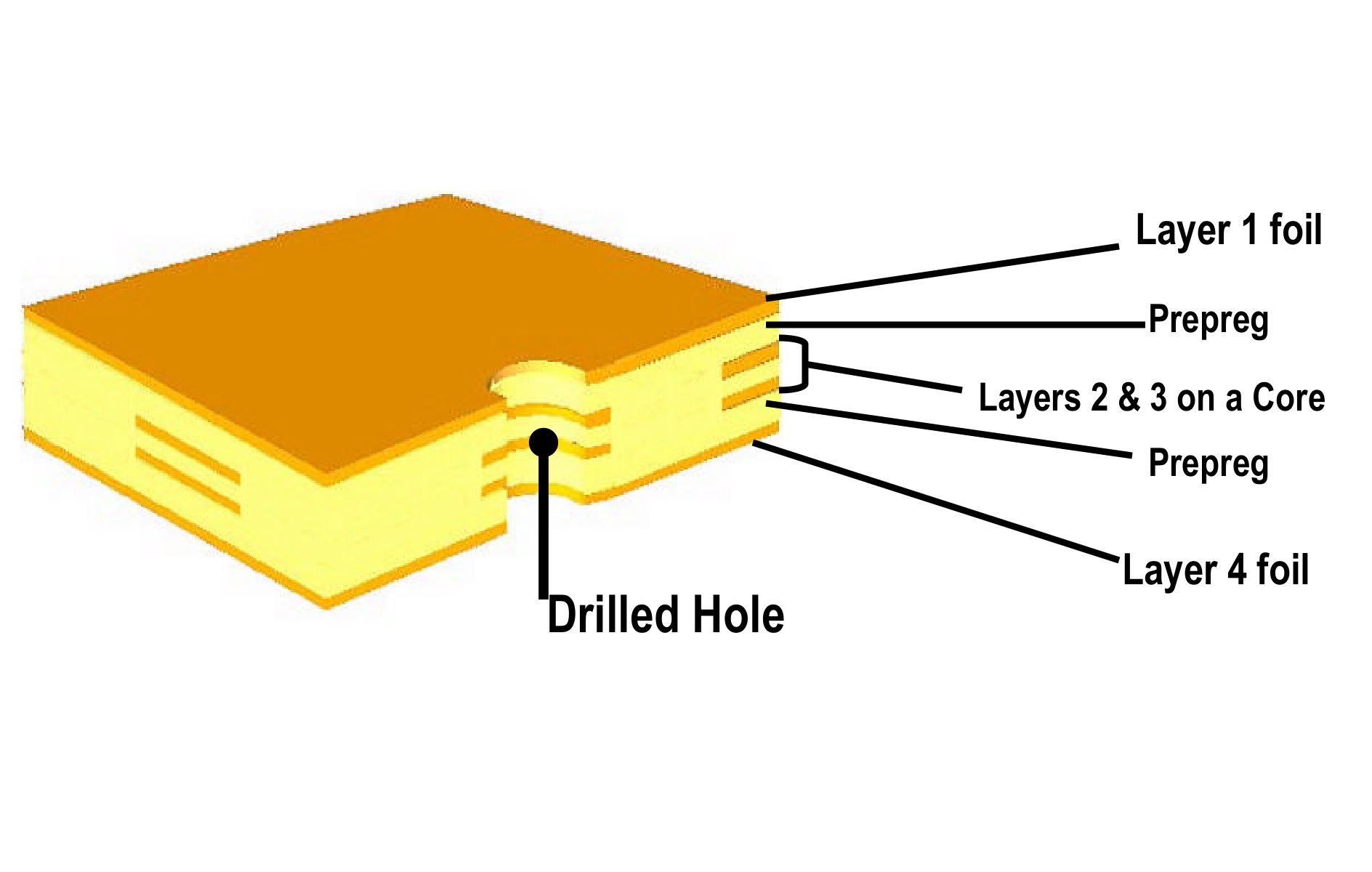
8. Lamination
This equipment is used to press PCB inner cores, prepregs and copper foils together to be multilayer PCB panels. It features hot oil heated beds with vacuum for outgassing. Load systems move the panels from the hot presses to the cold press/cool down stages of the process. The entire lamination process is computer controlled.
9. Drilling
Drilling is very critical to the PCB manufacturing process, holes of various sizes are drilled through a stack of working panels and the drilling process is computer numerical control.
10. PTH (Plated through hole)
In order for the through holes to electrically connect to different layers of the PCB, a thin layer of copper is chemically deposited into the through holes and on the surface of copper, this copper will later be thickened through pattern plating process.
11. Automatic Dry Flim laminator for outer layer image
The panels continue directly into the Clean Room passing through the auto-laminator receiving dry film Photo-resist for the outer layer imaging process. Again this type of automation reduces time and increases the quality and overall efficiency of the process.
12. Outer Layer Expose & Develop
Outer layer image exposure is performed in another clean rooms which are temperature and humidity controlled, this expose process places outer layer images from artwork onto the drilled panel. Exposed panels exit our clean rooms feeding directly into IS developers that develop the photo resist. Panels are then moved to pattern plating (copper/tin plating).
13. Pattern plating
The electroplating processes that electrically plates copper onto the exposed metal surfaces, the copper will be plated up to a required thickness for the working panel. The copper plating step is followed by plating Tin onto all the exposed copper surfaces, the Tin will be used as an etch resist to maintain the copper traces, hole pads and walls during the outer layer etch process.
14. SES(Strip Film – Etch – Strip Tin)
SES process include three sections to complete, the first section is Strip Film, the second section is Etch, and the third section is Strip Tin
Strip Film: The developed dry film resist is now removed from the working panel. The Tin plating is not affected. Any holes that were covered with resist are now open and will be non-plated.
Etch: Copper is now removed from all parts of the panel that are not covered by Tin. The Tin resists the chemicals used to etch away the copper. Only the pads and traces from the artwork are left behind on the panel surface.
Strip Tin: The Tin is chemically removed leaving behind a bare copper and laminate panel. The surface pads, traces and palted through holes are the exposed copper.
15. Outer layer AOI ( Automated Optical Inspection)
Similar to inner layers, A-TECH carry out 100% AOI inspection for outer layer images to ensure that no any opens, shorts and reduced traces before printing solder mask ink.
16. Solder Mask Pre-treatment
The exposed copper surface pads, traces and plated through holes must be clean and free of oxidation prior to applying solder mask. During the cleaning process the surface is scrubbed with pumice to improve adhesion of the mask as well as to remove any surface contamination.
17. LPI Solder Mask
The working panels are coated completely by a photo-sensitive epoxy based ink. Using films and high intensity UL light we expose the solderable areas of the PCB. The main function of the solder mask is to protect the majority of the copper circuitry from oxidation, damage and corrosion as well as maintain isolation of the circuits during assembly.
18. Silkscreen
Ink is silkscreened onto one or both sides of the panel depending on the requirements. The printing usually dictates component placement, part number or name, data code, logo or other specified information.
19. Surface finish
Different kinds of surface finish as required are applied to the panels, this surface finish is used to protect the copper(solderable surfaces) from oxidation as well as act as a site for soldering of components to the PCB.
20. Profile
After surface finish the working panels are cut to size on CNC routing machines. Most panels have the individual parts routed out into single pieces or arrays of varying sizes. Boards or arrays can also be scored so that they can be easily broken apart after assembly.
21. Electrical test
Electrical test machine is used to detect opens or shorts if they exist before PCB shipment, It is insurance for the customer, that he will receive functional circuit board products and avoid the costly assembly of defect products. Normally we used flying probe test machine for PCB prototype and small quantity orders, but used E-Test fixture for large quantity/batch PCB orders which is more efficient.
22. FQC (Final Quality Control)
Every piece of boards are visually inspected to assure that they meet our customers' requirements, industry specifications and A-TECH CIRCUITS' standards, as well as having the physical dimensions and hole sizes verified.
23. Package and shipment
All the printed circuit boards meeting the acceptability standards are packed with vacuum inside and carton outside.
General inquiries & Customer Service
Tel: 86-755-2335 9039 | Fax: 86-755-3318 0939
E-Mail: Enquiry@atechcircuit.com
Skype: atechcircuits

Headquarters: 602, Building B3, Zhimei Huizhi Industrial Park, Fuyong Street, Bao'an District, Shenzhen City, China
Copyright © 2025 A-TECH CIRCUITS Co., Ltd. | All Rights Reserved
Hello, please leave your name and email here before chat online so that we won't miss your message and contact you smoothly.


