Latest products
A brief introduction to the six types of modules in PCB debugging technology
by:A-TECH
2021-03-28
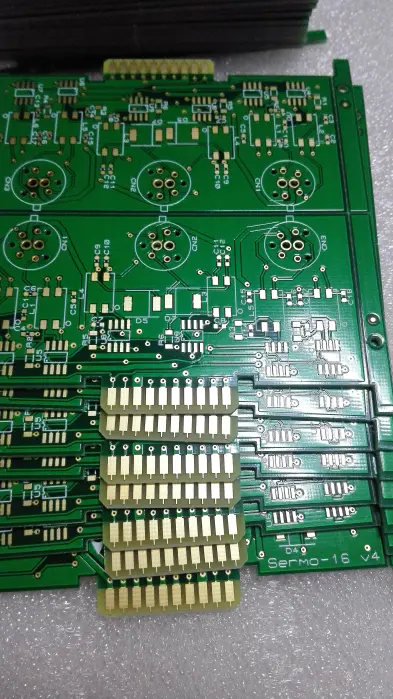
In the process of PCB copy board design, we often need to debug and test the circuit board. The debugging of the six types of modular circuit boards is one of them. In order to let everyone better understand the debugging technology of the six types of modular circuit boards, I Let me give you a brief introduction to the six types of modules. The core component of the six types of modules is the circuit board, and its design structure and manufacturing process basically determine the performance indicators of the product. The six types of modules implement the standard EIA/TIA 568B.2-1, and the most important parameter is the insertion loss. , Return loss, near-end crosstalk, etc. Insert Loss (Insert Loss): Due to the existence of the transmission channel impedance, it will increase the attenuation of the high-frequency components of the signal as the signal frequency increases. The attenuation is not only related to the signal frequency, but also related to the transmission distance. Increase, the signal attenuation will also increase. Return Loss: As the impedance changes in the product, local oscillations will occur, causing signal reflections. Part of the energy reflected to the transmitting end will form noise, leading to signal distortion and reducing transmission performance. For example, a full-duplex Gigabit network will mistake the reflected signal for the received signal and cause fluctuations in the useful signal, causing confusion. The less reflected energy, the better the impedance consistency of the line used in the channel, and the better the transmission The more complete the signal, the smaller the noise on the channel. The calculation formula of return loss RL: return lossu003dtransmitted signal÷reflected signal. In the entire design, ensuring the consistency of the impedance across the entire line and cooperating with the six types of cables with 100 ohm impedance is an effective means to solve the failure of return loss parameters. For example, the uneven distance between layers of the PCB circuit, the change of the copper conductor cross-section of the transmission line, the mismatch between the conductor in the module and the conductor of the six types of cables, etc., will cause the return loss parameter to change. Near-end crosstalk (NEXT): NEXT refers to the signal coupling of a pair of wires to another pair of wires in a pair of transmission lines, that is, when a pair of wires sends a signal, the signal is received on another adjacent pair of wires. signal. This kind of crosstalk signal is mainly due to the capacitive or inductive coupling of adjacent winding pairs. The main method to solve the failure of this parameter is to offset and weaken the interference signal through compensation. At the stage of module trial production, with theory as a guide and computer-aided design as the basis, the expected results can be quickly achieved. In the domestic PCB design of six types of modules, mainly based on the theory of line diagonal compensation, a large amount of trial production work is carried out, and the expected effect can also be achieved. The signal leakage caused by the module and the plug will cause mutual signal interference. In order to prevent signal interference, the conductors in the balanced link are twisted to achieve the purpose of balanced transmission. The twisted structure will cause the phase change between the signals. It will also increase the signal attenuation on the line. This structure is called an unshielded structure (UTP). In the 4 pairs of balanced twisted pairs, the lay length of each pair is different, and the modular connector is used at the end of the cable to form the connection between the connector and the connector, and the interconnection area forms a balanced structure between the conductors. , Which is the permanent link of the six types of systems. The signal interference phenomenon that occurs in the balanced line is generated in the permanent link, that is, crosstalk. Solving the crosstalk problem is the core technology for manufacturing high-speed communication connectors. The occurrence of contact loss between contact terminals can lead to phenomena such as attenuation and reflection loss. This loss can cause obstacles and failures during high-speed signal transmission. Solving such problems is the core technology for manufacturing high-speed communication connectors. In the connection line between the module and the plug, each pair of connecting terminals in the plug is a balanced line. The conductor in the balanced line will cause signal leakage and impedance loss. The biggest factor hindering communication is signal leakage. This type of problem can be solved by studying E-field and H-field, or a solution can be found from the method of studying reverse attenuation. This is the core technology for the manufacturing of high-speed communication connectors. The signal interference that occurs on the E-field and H-field balance line, that is, electromagnetic field interference, can be described by the distribution of E-field and H-field. The main parameter of the electronic communication circuit test is the relevant measurement under the frequency sweep. The voice or data packet is added to this frequency signal for transmission. The higher the transmission speed, the faster the frequency. Use the signal leakage solution to explain the socket signal leakage phenomenon that caused the problem. The most basic method is to collect the signal in the signal concentration area and send it back based on the simulation diagram of the signal leakage caused by the inductance and capacitance. In the design, the design of the coupling capacitor is a key parameter, which is related to the length of the coupling line, the distance between the lines, the width, and the layout of the compensation line. Taking into account that the six types of systems use 4 pairs of lines to transmit signals at the same time, it will inevitably produce comprehensive remote crosstalk. Through analysis and computer simulation, a compensation circuit can be designed. The six types of module trial production process generally carried out by domestic counterparts is mainly after determining the main circuit, designing the compensation circuit, and carrying out a large number of scheme designs and sample production. After the compensation circuit and the PCB interlayer structure are basically determined, the follow-up work is mainly through Process improvements to improve performance. The main adjustment parameters of the six types of module PCB debugging technology are: Interlayer gap parameters, copper foil thickness parameters, 8 main transmission line layout parameters, 8 main transmission lines width, relative distance; Adopt diagonal compensation method to adjust each line pair Compensation with other wire pairs, including compensation circuit position distribution, compensation circuit length and width, compensation circuit gap, etc.; adjustment of the process parameters of PCB processing plants; every circuit board design engineer and PCB copy board practitioners must master the six Class module PCB debugging technology and skills, only by mastering the six types of module PCB debugging technology, can we make a good quality circuit board, can get praise, and can stand in the market.
Custom message