Company Advantages1. The quality of A-TECH press fit pins pcb is guaranteed to meet the standards of the heatsink industry, including the safety and electricity performance standards. Its working panel is coated with a photo-sensitive epoxy-based ink, which can ensure its insulation resistance
2. It is a highly efficient product which is ideal for heat transfer in linear air-flow environments. Many customers have used it in their electronic products. With a solder mask, it enjoys a good electrical insulation property
3. The product is not susceptible to chemicals. The chromium element has been added as an agent to provide corrosion resistance. Its robust structure allows it to be used in harsh environments
4. The product has the advantage of chemical resistance. It can withstand the impacts of chemicals such as acids, salts, and alkalis. It has increased power densities which guarantee its long service life
5. This product features robustness. The metal material is well known for its robust property especially when exposed to strong impact, it is not easy to bend or crack. The product can be resistant to corrosion
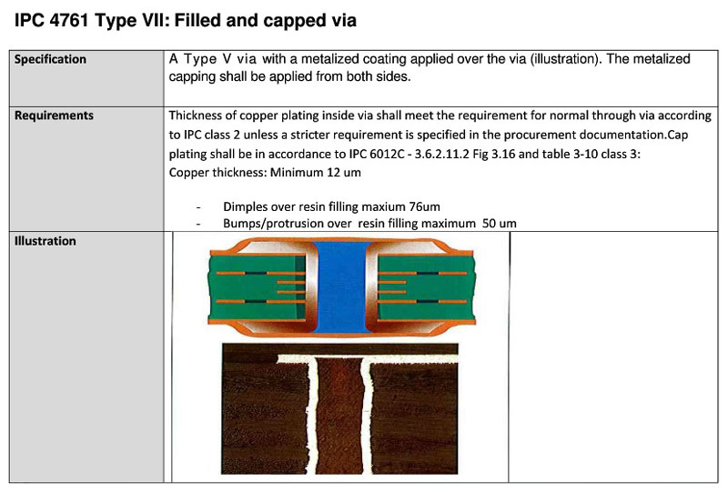
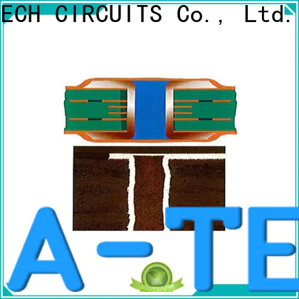
Via In Pad (VIP) technology refers to the vias in SMD pad or BGA pad due to small space for layout, in order to avoid the solder paste flow into inner layer or the other side in assembly production, basically this type of via need to be plugged with resin and plate copper over to cap the via to make it invisible.
Via in pad technology is widely used in high density PCBs, especially for the PCBs that require a limited BGA space and are focused on heat transfer and high speed design. Although blind holes and buried holes help increasing density and save space on the circuit boards, through holes are still the best choice for thermal management and high speed design elements.
The advantages of Via In Pad technology
● Suitable for fine pitch BGAs
● Improved thermal dissipation
● Provides a flat, coplanar surface for component attachment
● Leading to higher density of PCBs and promoting space saving
● Overcomes high speed design issues and constraints.
● Meets closely packed placement requirements.
The Via In Pad technology is defined in IPC standard with IPC-4761 VII

A-TECH manufactured lots of multilayer PCBs with Via In Pad designs Both in BGA Pads or in other SMD Pads, we’re able to plugged vias fully and then plated copper over to make the surface of pad as flat as other pads without dimples.
Company Features1. A-TECH CIRCUITS Co., Ltd. is known for its R&D capability and rich manufacturing experience in pcb plating . We have an export license issued by the National Foreign Trade and Economic Cooperation Administrative Department. The export license has enabled us to unlock the international market and expand the scope operation.
2. We have many loyal customers. Most of them have signed a long-term cooperation agreement with us. The pleasant cooperation with foreign customers has once again demonstrated our strength.
3. Our company makes use of advanced technology to the point of Simplicity and also focuses on great innovation in their products. The products carry great design that actually fits seamlessly into the requirement of the customers. We gear towards more sustainable business and environment development. We make efforts in introducing effectual sewage disposal and exhaust emission clean systems to minimize the adverse impact on our environment.


