
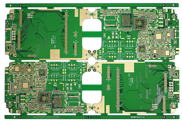
After PCB design wiring is completed, due to the requirements of PCB design and assembly process, some PCBs with special shapes need to be designed together, so that the subsequent PCB assembly process can proceed smoothly. When designing a panelization, it is usually necessary to add side bars, and connect one or several PCB units and side bars together in a certain way to form a PCB shape that meets the assembly requirements. The size of the panel will have a direct impact on the material utilization rate and the size of the panel produced during PCB production, and even significantly affect the price of PCB. The number, width, position, number of PCB units, arrangement of PCB units, connection methods, and slot width in the panelization will all affect the size of the panelization.
This article mainly discusses how to optimize the size of the panel by controlling these influencing factors under the premise of meeting the PCB and PCB assembly process requirements in the process of panel design, so that it can produce high plate utilization when forming PCB production panels Rate and suitable production panel size, so as to obtain a lower PCB quotation.
The situation that pcb has to do a panelization
In the following cases, the PCB needs to be assembled to form a panel to meet the PCB assembly process requirements:
(1) The mechanical structure requirements of the PCB design itself
(2) The component pads are too close to the edge of the PCB board, the top layer is less than 4.06 mm, and the bottom layer is less than 5.08 mm (the top layer is less than 0.16 inches and the bottom layer is less than 0.2 inches)
(3) The test points that require soldering are too close to the board edge, the top layer is less than 4.06 mm, and the bottom layer is less than 5.08 mm (the top layer is less than 0.16 inches and the bottom layer is less than 0.2 inches)
(4) Irregular shape or size is too small to pass the assembly line smoothly
(5) To improve the efficiency of PCB assembly production process
Assemble strictly in accordance with the PCB design process, which can greatly save costs and achieve more ideal PCB board production results.
General inquiries & Customer Service
Tel: 86-755-2335 9039 | Fax: 86-755-3318 0939
E-Mail: Enquiry@atechcircuit.com
Skype: atechcircuits

Headquarters: 602, Building B3, Zhimei Huizhi Industrial Park, Fuyong Street, Bao'an District, Shenzhen City, China
Copyright © 2025 A-TECH CIRCUITS Co., Ltd. | All Rights Reserved
Hello, please leave your name and email here before chat online so that we won't miss your message and contact you smoothly.


