What Is Osp Surface Finish?and Are The Advantages
by:A-TECH
2020-09-02
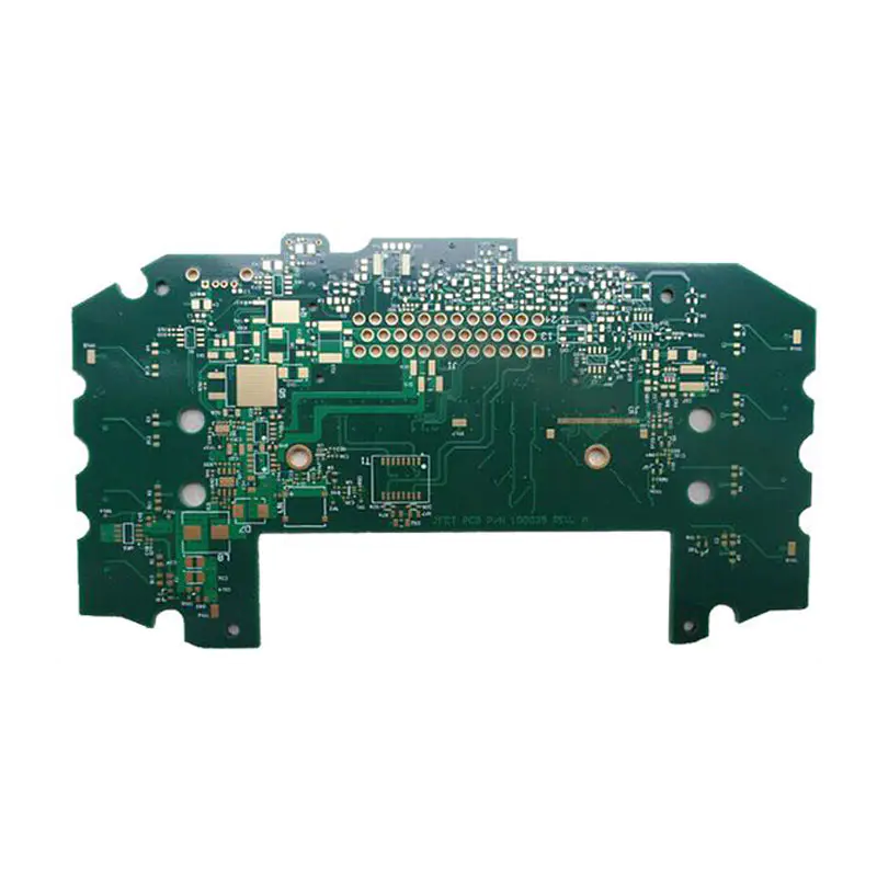
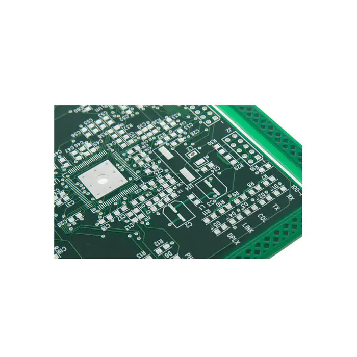
A PCB could also be 'silkscreen' printed with a legend identifying the parts, test points, or identifying textual content. Originally, an actual silkscreen printing process was used for this function, but today other, finer high quality printing methods are often used as an alternative. Normally the display screen printing is not significant to the function of the PCBA. Whether you need a simple single-layer PCB or an extremely complex 30-layer multi-layer PCB, PCBCart can make your concepts a actuality.
Metal-core boards for high energy units commonly use thicker copper; 35 µm is usual but in addition one hundred forty and 400 µm may be encountered. Loss tangent determines how much of the electromagnetic energy from the alerts in the conductors is absorbed in the board material. Choosing unnecessarily low-loss material is a standard engineering error in high-frequency digital design; it increases the cost of the boards with no corresponding profit. Signal degradation by loss tangent and dielectric constant can be easily assessed by an eye fixed sample.
Trace separation is also taken under consideration in case of differential signals. Microstrip, stripline or twin stripline can be utilized to route signals.
In bubble etching, air is handed through the etchant bath to agitate the answer and speed up etching. Splash etching makes use of a motor-pushed paddle to splash boards with etchant; the method has turn into commercially out of date since it's not as fast as spray etching. In spray etching, the etchant resolution is distributed over the boards by nozzles, and recirculated by pumps. Adjustment of the nozzle sample, move price, temperature, and etchant composition offers predictable control of etching rates and excessive production rates. Line impedance is determined using dielectric layer thickness, routing copper thickness and trace-width.
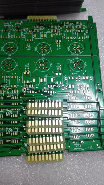
Safety Standard UL 796 covers part security requirements for printed wiring boards to be used as parts in gadgets or appliances. Testing analyzes traits corresponding to flammability, maximum working temperature, electrical monitoring, heat deflection, and direct support of stay electrical components. On the common FR-four substrates, 1 oz copper per ft2 (35 µm) is the most typical thickness; 2 oz (70 µm) and zero.5 oz (18 µm) thickness is usually an choice. Less common are 12 and a hundred and five µm, 9 µm is typically available on some substrates.
Custom message