
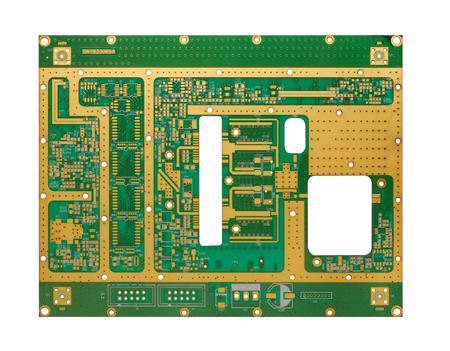
Definition of high-frequency pcb board made by circuit board. High-frequency board refers to a special circuit board with high electromagnetic frequency, which is used in the field of high frequency (frequency greater than 300MHZ or wavelength less than 1 meter) and microwave (frequency greater than 3GHZ or wavelength less than 0.1 meter) PCB is a circuit board produced on microwave substrate copper-clad board using part of the process of ordinary rigid PCB manufacturing method or using special processing methods. Generally speaking, high-frequency boards can be defined as circuit boards with frequencies above 1GHz.
With the rapid development of science and technology, more and more equipment designs are applied in the microwave frequency band (> 1GHZ) and even in the field of millimeter wave (30GHZ), which also means that the frequency is getting higher and higher. The requirements for timber are also increasing. For example, the substrate material needs to have excellent electrical properties, good chemical stability, and the loss on the substrate as the frequency of the power signal increases is very small, so the importance of high-frequency plates is highlighted.
PCB high-frequency board application field mobile communication products; power amplifiers, low-noise amplifiers, etc .; passive devices such as power dividers, couplers, duplexers, filters; automotive anti-collision systems, satellite systems, radio systems, etc. The high frequency of equipment is the development trend.
PCB high-frequency board application field mobile communication products; power amplifiers, low-noise amplifiers, etc .; passive devices such as power dividers, couplers, duplexers, filters; automotive anti-collision systems, satellite systems, radio systems, etc. The high frequency of equipment is the development trend.
Summarize the difficult points of circuit board high frequency board processing
1. Copper plated: the hole wall is not easy to be copper plated
2. Control of image transfer, etching, line width line gap, sand hole
3. Solder mask process: control of solder mask ink adhesion and ink foaming
4. Strict control of scratches on the board surface occurs in each process.
General inquiries & Customer Service
Tel: 86-755-2335 9039 | Fax: 86-755-3318 0939
E-Mail: Enquiry@atechcircuit.com
Skype: atechcircuits

Headquarters: 602, Building B3, Zhimei Huizhi Industrial Park, Fuyong Street, Bao'an District, Shenzhen City, China
Copyright © 2025 A-TECH CIRCUITS Co., Ltd. | All Rights Reserved
Hello, please leave your name and email here before chat online so that we won't miss your message and contact you smoothly.


