
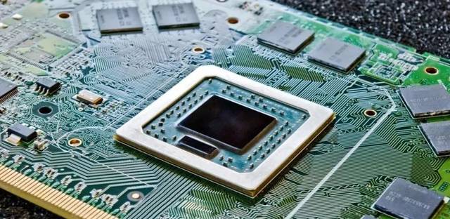
BGA is a packaging method. The full name of BGA is Ball Grid Array. With the continuous development of electronic technology in the 1990s, the IC processing speed has also continued to increase. The number of I / O pins on integrated circuit chips has increased. Continuous improvement, all levels of elements clearly put forward higher regulations on IC packaging, and in order to consider the development of electronic equipment towards miniaturization and precision, BGA packaging has been released and put into production.
The factors affect BGA assembly:
In the specific SMT patch processing, the thickness of the steel mesh is generally 0.12mm, but the thick steel mesh in the welding process of the BGA device is likely to lead to tin. According to the experience of assembly production work, the steel mesh with a thickness of 0.1mm BGA devices are very suitable, in addition, it can also moderately expand the total area of the steel mesh opening.
2. Solder paste
The pin spacing of BGA devices is relatively small, so the solder paste used also stipulates that the metal material particles should be small. Excessive metal material particles will cause continuous tin in SMT processing.
3. Welding temperature setting
The reflow soldering furnace is generally used in the entire process of SMT placement. Before welding for BGA packaged components, the temperature of each region must be set according to the processing regulations and the temperature around the spot welding must be detected using a thermal resistance camera.
4. Inspection after welding
After PCB SMT processing, we must carry out rigorous testing of BGA packaged devices to prevent some chip-type defects.
5. Advantages of BGA packaging:
5.1. Increased assembly yield;
5.2. The electric heating performance is improved;
5.3. The volume and mass are reduced;
5.4. The parasitic parameters are reduced;
5.5. The signal transmission delay is small;
6.6. Increased frequency of use;
7.7. Good product credibility;
6. Defects of BGA packaging:
6.1. Inspection after welding must be based on X-ray;
6.2. Increased production cost of electronics;
6.3. Increased cost of repairs;
General inquiries & Customer Service
Tel: 86-755-2335 9039 | Fax: 86-755-3318 0939
E-Mail: Enquiry@atechcircuit.com
Skype: atechcircuits

Headquarters: 602, Building B3, Zhimei Huizhi Industrial Park, Fuyong Street, Bao'an District, Shenzhen City, China
Copyright © 2025 A-TECH CIRCUITS Co., Ltd. | All Rights Reserved
Hello, please leave your name and email here before chat online so that we won't miss your message and contact you smoothly.


