
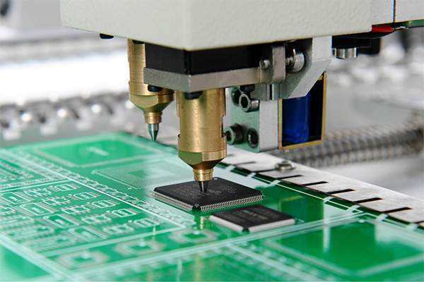
PCB soldering technology has made great progress in the electronics industry in recent years, and it can be noted that a very obvious trend is the problem of reflow soldering technology. The quality of PCB circuit board soldering is also a matter of close attention of major electronic manufacturers. Let's take a look at the three major factors that constitute PCB board soldering defects!
1. The solderability of PCB board holes affects the welding quality
PCB board hole solderability is not good, will produce virtual soldering defects, affecting the parameters of the circuit components, resulting in unstable conduction of the multilayer board components and inner line, causing the entire circuit function failure. The so-called solderability is the property of the surface of the metal being wetted by the molten solder, that is, the surface of the metal where the solder is located constitutes a relatively even continuous lubricating adhesion film.
2. Soldering defects caused by PCB board warpage
The PCB board and components are warped during the welding process, and defects such as virtual welding and short circuit are generated due to stress and deformation. Warpage is often caused by the uneven temperature of the upper and lower parts of the PCB. For large-size PCB boards, due to their own weight, they will also warp. Ordinary PBGA devices are about 0.5mm apart from the PCB board. Assuming that the PCB board is larger, the solder joint will be under stress for a long time as the PCB board cools down, assuming that the device is raised by 0.1mm is enough to cause false Welding open.
3. The design of the PCB board affects the welding quality
In the planning, when the PCB board size is too large, although the soldering is easier to control, but the printed lines are long, the impedance increases, the ability to resist noise drops, the cost increases; if it is too small, the heat dissipation drops, the soldering is not easy to control, and the adjacent lines are easy to show Mutual interference, such as the electromagnetic interference of the PCB board. Therefore, it is necessary to optimize the PCB board design. For factories that fail to meet the technical requirements, PCB outsourcing can be used to solve the problem.
General inquiries & Customer Service
Tel: 86-755-2335 9039 | Fax: 86-755-3318 0939
E-Mail: Enquiry@atechcircuit.com
Skype: atechcircuits

Headquarters: 602, Building B3, Zhimei Huizhi Industrial Park, Fuyong Street, Bao'an District, Shenzhen City, China
Copyright © 2025 A-TECH CIRCUITS Co., Ltd. | All Rights Reserved
Hello, please leave your name and email here before chat online so that we won't miss your message and contact you smoothly.


