Latest products
What design principles should PCB circuit boards follow?
by:A-TECH
2021-03-11
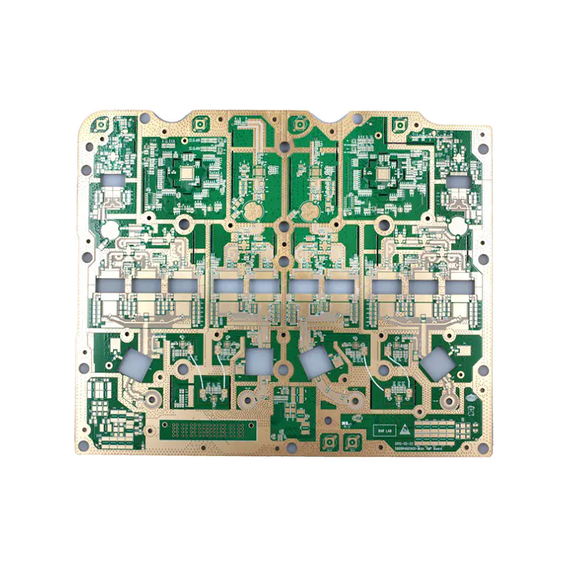
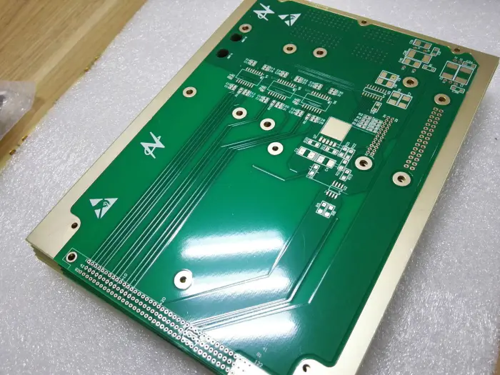
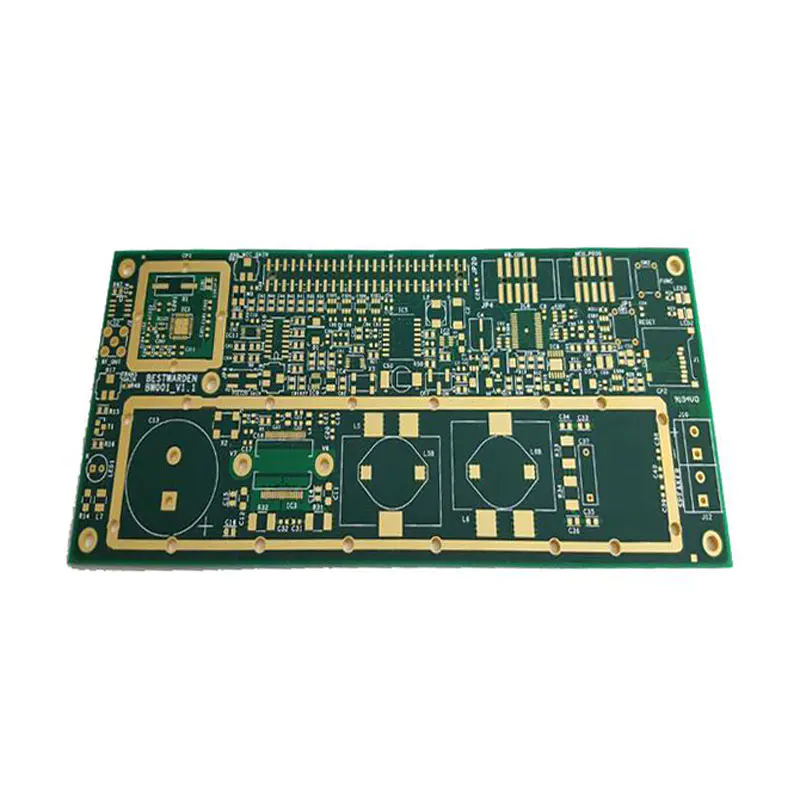
In today's highly developed technology, the upgrading of electronic products is getting faster and faster. Practice has proved that even if the circuit schematic is designed correctly and the printed circuit board is not properly designed, it will adversely affect the reliability of electronic equipment. So, what design principles should the PCB circuit board follow? 1. Ground wire design In electronic equipment, grounding is an important method to control interference. If the grounding and shielding can be properly combined and used, most interference problems can be solved. Pay attention to the following points in the ground wire design: (1) Correctly choose single-point grounding and multi-point grounding; (2) Separate the digital circuit from the analog circuit; (3) Thicken the ground wire as much as possible; (4) Connect the ground wire Form a closed loop. 2. Electromagnetic compatibility design The purpose of electromagnetic compatibility design is to enable electronic equipment to suppress all kinds of external interference, so that electronic equipment can work normally in a specific electromagnetic environment, and at the same time to reduce the electronic equipment itself to other electronic equipment. Electromagnetic interference. (1) Choose a reasonable wire width. The inductance of the printed wire is proportional to its length and inversely proportional to its width. Therefore, a short and precise wire is beneficial to suppress interference. (2) Adopting the correct wiring strategy and using equal wiring can reduce the wire inductance, but the mutual inductance and distributed capacitance between the wires will increase; if the layout permits, it is best to use a tic-tac-toe mesh wiring structure. (3) Suppressing reflection interference In order to suppress the reflection interference appearing at the printed line terminal, in addition to special needs, the length of the printed line should be shortened as much as possible and a slow circuit should be used. 3. The decoupling capacitor is configured in the DC power loop, and the change of the load will cause power noise. The configuration of decoupling capacitors can suppress noise caused by load changes. 4. The size of the printed circuit board and the configuration of the components are the same as other logic circuits in terms of component layout. The components related to each other should be placed as close as possible to obtain a better anti-noise effect. Noise-prone devices, low-current circuits, and high-current circuits should be kept away from logic circuits as much as possible. 5. Thermal design From the perspective of conducive to heat dissipation, the printed plate is best installed upright, and the distance between the board and the board should generally not be less than 2cm. A lot of practical experience shows that using a reasonable device arrangement can effectively reduce the temperature rise of the printed circuit. The above are the design principles that PCB circuit boards should follow. How much do you know?
Custom message