SMT plug-in processing of large size BGA corners of the reinforcement
by:A-TECH
2020-05-21
SMT plug-in processing of large size BGA corners of the reinforcement.
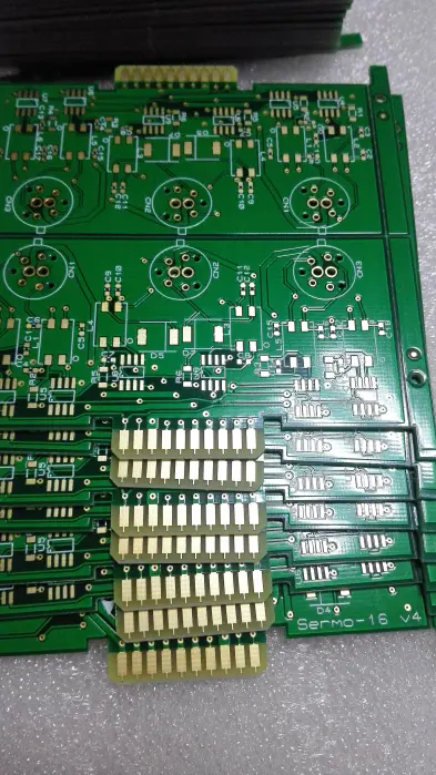
PCBA bending, BGA location in the four corners of the solder joint stress, RongSheng cracked or broken.
For this, keep strengthening of BGA corners, to prevent cracking Angle welds is very reasonable, should choose a special glue to do reinforcement, also can choose patch rubber reinforcement.
It's stipulated components out of time and space space layout, reinforce the standards and ways in process documents marked.
Remove from SMT plug-in processing of solder surface oxide or other contaminants.
Prior to welding the main task of the SMT chip processing from solder surface to remove oxides.
Within the scope of the activation temperature, flux of rosin acid will stay with the oxide film on the surface of the weld metal are restored, and forming a copper rosin acid.
The rosin acid easy to mix with don't participate in the reaction of rosin, and keep on bare copper surface, in order to make the solder flow.
Wet.
Flux of the surfactant and copper oxide reaction, eventually instead of pure copper.
Flux of metal salts and to the surface of the weld metal oxide substitution reaction.
Flux of organic halide will react with the metal surface, for welding to remove oxides.
Rely on optics instrument calibration, the size of the ultraviolet laser beam can reach 10 -
20 microns, thus producing flexible circuit trace.
Figure 2 shows that the application of ultraviolet ray trace in the production of circuit advantages, circuit tracing line is extremely small, need to under a microscope to see.
This circuit board size is zero.
75 - inch x0.
5 inches, by a sintering ceramic substrate and tungsten/nickel/copper/surface composition.
Laser can produce 2 mils circuit trace spacing of 1 mil, making the entire spacing for only 3 mils.
Custom message