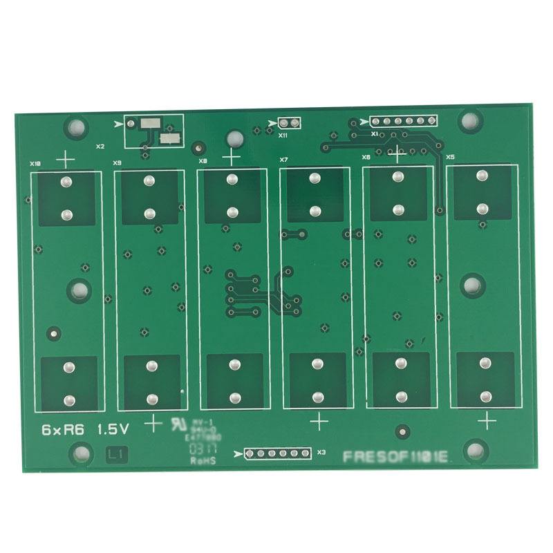
In double-sided and multi-layer PCB boards, in order to connect the printed wires between the layers, a common hole is opened at the intersection of the wires that need to be connected, but pay attention to the outer diameter of the hole and the size of the hole This is a via, also known as a metalized hole. There are three types of via processing methods: via solder mask opening, via ink cover, and via ink plugged. Let's talk about the definition of via plug ink.

Through-hole plug ink is to guide the hole through the hole to make the plug hole with ink, emphasizing the quality and density of the plug hole. The inspection standard for the treatment of via plug ink is to be opaque, and it must be covered and blocked with ink. The second is that the orifice must not be yellowed, and it must be free of tin. The via plug ink process is an important supplement to the via cap ink. Generally, high-quality PCB boards are required to be made into via plug ink. The via plug ink first plugs the entire hole of the via hole with ink, and the plug hole cannot be transparent to block the via hole, so that the ink on the solder resist ring will not flow into the via hole, so that the via hole does not yellow effect. The smaller the via hole, the easier it is to plug. The via hole of the fortress ink is not easy to be too large, the maximum is 0.5mm, so the hole larger than 0.5mm is recommended to cover the via ink.
The vias mentioned above are usually used for interlayer conduction. Therefore, in order to avoid short circuit and other situations when the board is used, cover ink is usually used, which not only ensures the electrical performance, but also avoids the risk of short circuit with other components during use. Will open the solder mask window.
Copyright © 2025 A-TECH CIRCUITS Co., Ltd. | All Rights Reserved
Hello, please leave your name and email here before chat online so that we won't miss your message and contact you smoothly.