
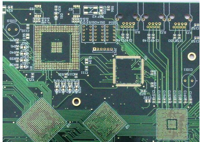
PCB using resin plug holes This process is often because of BGA parts, because traditional BGA may do VIA between PAD and PAD to the back to route, but if the BGA is too dense, When you can't go out, you can directly drill holes from the PAD to go to another layer, and then fill the holes with resin to form copper plating to become PAD, also known as the VIP process (via in pad PCB). If you only do vias on the PAD without using resin plug holes, it is easy to cause tin leakage and lead to short circuit on the back and empty welding on the front.
The PCB manufacturing process with resin plug holes includes drilling, electroplating, plug holes, baking, and grinding. After drilling, the holes are plated through, and then the resin is baked, and finally the grinding is to smooth it out and grind. The flat resin does not contain copper, so it needs another layer of copper to turn it into PAD. These processes are done before the original PCB drilling process, that is, the fortress hole is first. The holes are processed, and then drill other holes, and follow the original normal process.
If the plug hole is not plugged well, if there are bubbles in the hole, because the bubbles are easy to absorb moisture, the board may burst when passing through the tin furnace again, but if there are bubbles in the hole during the plug hole process, bake Bubbles will squeeze out the resin, causing depression and protruding. At this time, the defective product can be detected, and the board with bubbles may not necessarily burst, because the burst the main reason is the moisture, so if the board or the board has just been baked when it was shipped, generally it will not cause a burst.
General inquiries & Customer Service
Tel: 86-755-2335 9039 | Fax: 86-755-3318 0939
E-Mail: Enquiry@atechcircuit.com
Skype: atechcircuits

Headquarters: 602, Building B3, Zhimei Huizhi Industrial Park, Fuyong Street, Bao'an District, Shenzhen City, China
Copyright © 2025 A-TECH CIRCUITS Co., Ltd. | All Rights Reserved
Hello, please leave your name and email here before chat online so that we won't miss your message and contact you smoothly.


