
With the rapid development of electronic products, high-density multi-function miniaturization has become the development direction. The components on the printed circuit board are increasing in geometric index, but the size of the circuit board is constantly decreasing, and it is often necessary to match some small carrier boards. If the round hole of the small carrier board is soldered to the mother circuit board with solder, due to the large volume of the round hole and the problem of virtual soldering, the child and mother printed circuit boards cannot be well connected electrically, so a metallization half hole PCB. The characteristics of the metallized half hole PCB are: the individual is relatively small, and the unit has a row of metallized semi-holes. Welded together.
Difficulties in metallized half-hole PCB processing:
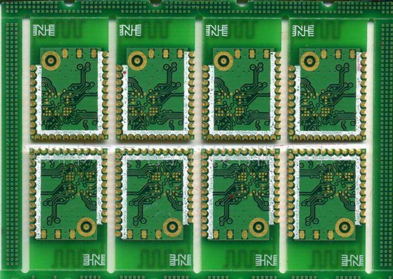
After the metallized half hole PCB is formed, the copper wall of the hole wall is black, the burrs fall, and the deviation is always a problem in the molding process of each PCB factory. In particular, the entire row of semi-holes that resemble stamp holes has an aperture of about 0.6mm, the hole wall spacing is 0.45mm, and the outer layer spacing is 2mm. Because the spacing is very small, it is easy to cause a short circuit due to copper skin.
The general processing methods of metallized half-hole board PCB molding include CNC milling machine gong board, mechanical punching, VCUT cutting, etc. These processing methods will inevitably lead to the remaining part when removing the copper that does not require part of the hole Copper wire and burrs remain on the cross-section of the PTH hole, and there is a serious phenomenon that the copper wall of the hole wall is warped and peeled. On the other hand, when forming the metallized half-holes, due to the influence of PCB expansion and contraction, drilling hole position accuracy, and molding accuracy, the size deviation of the left and right half holes on the left and right sides of the same unit during the molding process is large, which gives customers welding assembly tape To greatly trouble.
Traditional metallized half-hole plate production process:
Drilling—chemical copper—full-plate copper—image transfer—graphic plating—removal of film—etching—solder masking—half holes on the surface (formed simultaneously with the shape).
This metallized half-hole is formed by cutting the round hole in half after the round hole is formed. It is easy for the phenomenon of residual half-hole copper wire and copper skin to lift up, which affects the function of the half hole, resulting in a decline in product performance and yield. In order to overcome the above shortcomings, the following metallized semi-orifice PCB process steps should be followed:
After the substrate is subjected to secondary copper plating and tin plating, the circular hole on the edge of the board is cut in half to form a half hole. Because the copper layer on the hole wall is covered with a tin layer, and the copper layer on the hole wall is completely connected with the copper on the outer layer of the substrate, It has large binding force, which can effectively prevent the copper layer on the hole wall from being pulled off or copper lifting when cutting;
After the half-hole plate is formed, the film is removed, and then the etching is performed, and the copper surface oxidation will not occur, which effectively avoids the occurrence of residual copper or even short circuit, and improves the yield of the metallized half-hole plate PCB circuit board.
General inquiries & Customer Service
Tel: 86-755-2335 9039 | Fax: 86-755-3318 0939
E-Mail: Enquiry@atechcircuit.com
Skype: atechcircuits

Headquarters: 602, Building B3, Zhimei Huizhi Industrial Park, Fuyong Street, Bao'an District, Shenzhen City, China
Copyright © 2025 A-TECH CIRCUITS Co., Ltd. | All Rights Reserved
Hello, please leave your name and email here before chat online so that we won't miss your message and contact you smoothly.


