
The double-sided circuit board is the middle layer of dielectric, and both sides are trace layers. A multi-layer circuit board is a multi-layer wiring layer. Between each two layers is a dielectric layer, which can be made very thin. The multilayer circuit board has at least three conductive layers, two of which are on the outer surface, and the remaining layer is synthesized in the insulating board. The electrical connection between them is usually achieved through plated through holes on the cross section of the circuit board.
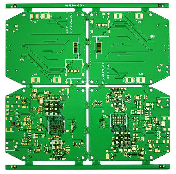
The multilayer PCB circuit board is a printed circuit board formed by laminating and bonding alternating conductive pattern layers and insulating materials. The number of layers of the conductive pattern is more than three layers, and the electrical interconnection between the layers is realized by metallized holes. If one double-sided board is used as the inner layer, two single-sided boards are used as the outer layer, or two double-sided boards are used as the inner layer, and two single-sided boards are used as the outer layer, the conductive pattern is laminated according to the positioning system and insulating bonding material The design requires interconnection to become a four-layer or six-layer printed circuit board, also known as a multilayer PCB circuit board.
Compared with the general production process of multilayer pcb boards and double-sided pcb boards, the main difference is that multilayer boards add several unique process steps: inner layer imaging and blackening, lamination, etchback and decontamination. In most of the same processes, some process parameters, equipment accuracy and complexity are also different. For example, the inner metallization connection of the multi-layer board is a decisive factor for the reliability of the multi-layer board. The quality of the hole wall is stricter than that of the double-layer board, so the requirements for drilling are higher. In addition, the number of stacked plates for each drilling of the multilayer board, the speed of rotation and the feed rate of the drill during drilling are different from those of the double-sided board. The inspection of finished and semi-finished multi-layer boards is also much stricter and more complicated than double-sided boards.
Advantages and disadvantages of multilayer circuit boards
advantage:
High assembly density, small size, light weight. Due to high assembly density, the wiring between components (including components) is reduced, so reliability is improved; the number of wiring layers can be increased, thereby increasing design flexibility; Circuits with a certain impedance; high-speed transmission circuits can be formed; circuit, magnetic circuit shielding layers can be set, and metal core heat dissipation layers can also be set to meet the needs of special functions such as shielding and heat dissipation; simple installation and high reliability.
Disadvantages:
High cost; long cycle; high-reliability testing methods are required. Multilayer printed circuit is the product of the development of electronic technology towards high speed, multi-function, large capacity and small volume. With the continuous development of electronic technology, especially the extensive and in-depth application of large-scale and ultra-large-scale integrated circuits, multilayer printed circuits are rapidly developing into high-density, high-precision, high-level digitalization. Fine lines, small apertures, Technologies such as blind hole embedding and high thickness-to-thickness ratio can meet the needs of the market.
General inquiries & Customer Service
Tel: 86-755-2335 9039 | Fax: 86-755-3318 0939
E-Mail: Enquiry@atechcircuit.com
Skype: atechcircuits

Headquarters: 602, Building B3, Zhimei Huizhi Industrial Park, Fuyong Street, Bao'an District, Shenzhen City, China
Copyright © 2025 A-TECH CIRCUITS Co., Ltd. | All Rights Reserved
Hello, please leave your name and email here before chat online so that we won't miss your message and contact you smoothly.


