
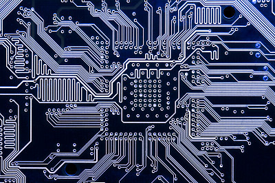
The printed circuit board is formed by stacking layers of copper foil circuits, and the connection between different circuit layers is through vias. This is because the current manufacturing of circuit board uses drill holes to communicate with different In the circuit layer, the purpose of the connection is to conduct electricity, so it is called a via. In order to conduct electricity, a layer of conductive material (usually copper) must be plated on the surface of the drilled hole, so that the electrons can be in different Move between the copper foil layers because the surface of the original drilled hole is not conductive only with resin.
Generally, there are three kinds of PCB vias (Via) that we often see in PCB fabrication, which are described as follows:
Through Hole: Plating Through Hole (PTH)
This is the most common kind of via hole. As long as you hold the PCB against the light, the hole where you can see the bright light is the "through hole." This is also the simplest kind of hole, because it only needs to use a drill or laser to directly drill the circuit board, and the cost is relatively cheap. Although vias are cheap, sometimes they use more PCB space. For example, we have a six-story house. I bought its third and fourth floors. I want to design a staircase inside to connect only the third and fourth floors. For me, the space on the fourth floor The staircase that was originally connected from the first floor to the sixth floor used up some space.
Blind hole: Blind Via Hole (BVH)
The outermost circuit of the PCB is connected to the adjacent inner layer with plated holes. Because the opposite side cannot be seen, it is called a "blind hole". In order to increase the space utilization of the PCB circuit layer, a "blind via" process was born. This manufacturing method requires special attention to the depth of the drill hole (Z axis) to be just right. You can drill the holes of the circuit layers that need to be connected in the individual circuit layers in advance, and then glue them together, but more precise positioning is required. And alignment device. Take the example of buying a building above. A six-story house only has a staircase that connects the first and second floors, or from the fifth floor to the sixth floor, which is called a blind hole.
Buried hole: Buried Via Hole (BVH)
The connection of any circuit layer inside the PCB but does not lead to the outer layer. This process cannot be achieved by drilling after bonding. Drilling must be performed on individual circuit layers. After the inner layer is partially bonded, it must be plated first before it can be fully bonded. "Blind hole" takes more time, so the price is also the most expensive. This process is usually only used on high-density (HDI PCB) circuit boards to increase the usable space of other circuit layers. Taking the example of buying a building above, a six-story house has only stairs connecting the third and fourth floors, which is called a buried hole.
General inquiries & Customer Service
Tel: 86-755-2335 9039 | Fax: 86-755-3318 0939
E-Mail: Enquiry@atechcircuit.com
Skype: atechcircuits

Headquarters: 602, Building B3, Zhimei Huizhi Industrial Park, Fuyong Street, Bao'an District, Shenzhen City, China
Copyright © 2025 A-TECH CIRCUITS Co., Ltd. | All Rights Reserved
Hello, please leave your name and email here before chat online so that we won't miss your message and contact you smoothly.


