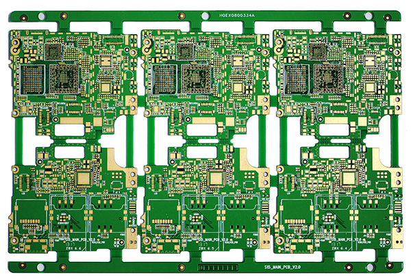
In high-speed PCB design, seemingly simple vias also often bring great negative effects to circuit design. In order to reduce the adverse effects caused by the parasitic effects of vias, in the design, you can do as much as possible:

1. From the two aspects of cost and signal quality, choose a reasonable size of via size. If necessary, you can consider using different sizes of vias. For example, for power or ground vias, you can consider using larger sizes to reduce impedance. For signal traces, you can use smaller vias. Of course, as the via size decreases, the corresponding cost will increase.
2. The two formulas discussed above can be concluded that the use of thinner PCB boards is beneficial to reduce the two parasitic parameters of vias.
3. The signal traces on the PCB board should not change layers as much as possible, that is to say, try not to use unnecessary vias.
4. The power and ground pins should be drilled through the hole. The shorter the lead between the hole and the pin, the better. You can consider making multiple vias in parallel to reduce the equivalent inductance.
5. Place some grounded vias near the vias for signal changeover to provide the closest loop for the signal. You can even place some extra ground vias on the PCB.
6. For high-density PCB and high-speed PCB boards, consider using micro vias.
Copyright © 2025 A-TECH CIRCUITS Co., Ltd. | All Rights Reserved
Hello, please leave your name and email here before chat online so that we won't miss your message and contact you smoothly.