Latest products
Circuit board manufacturing process
by:A-TECH
2020-05-14
The 4 layer board manufacturing process (
1)
Draw the film using Laser photo plotters,
Laser plotter)
, providing the manufacturing film, resistance welding layer film, printing film production engineering must be in the film, etc.
Wiring film.
Film in the process of adhesion, the number of run out error, especially for special process, the error is bigger.
So should fully consider problems in circuit preset to the effects of these errors, make reasonable default.
(
2)
Sheet metal cutting sheet metal production circuit board in the size of the factory is 1 m * 1 m or 1 m * 1.
2m。
Produce according to the demand of cut into different size of workpiece,
工作)
Volume of PCB, according to the preset to choose established workpiece size, prevent lead to cost, increase the cost of not essential.
(
3)
The inner circuit of forming next, form the inner circuit wiring)
。
With photosensitive dry film (
干膜)
Adhesion to as inner double coin, tiejin used in the manufacture of the inner line of the film, exposure, and imaging disposal, leaving only needed to get the line.
To implement on the both sides of the project after a rotten ke (
(
蚀刻)
)
Device to remove without copper foil.
Figure 8 1 ~ 5.
(
4)
Oxygen treatment (
Black disposal)
Before and outer synthesis, copper foil to oxygen disposal form tiny bump appearance.
It's also in order to increase the insulation and adhesion of half curing agent (
prepreg)
And the contact plane between the inner or the size of the object surface, make better adhesion.
Now in order to reduce background contamination, oxygen is developed by disposal of replacement products, and now have circuit sheet itself is good sex.
(
5)
Laminated treatment of laminated disposal 6 as shown in figure 8, oxygen through the disposal of the inner circuit, spread half curing agent, with the outer plate.
Under the vacuum condition, heating and execute compression after laminating machine.
Half a curing agent on the adhesion and utility of the insulation.
By laminated disposal, and double coin purposely look the same, since this project and two copper project also.
(
6)
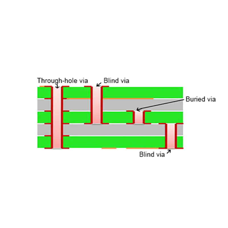
Opening numerical control machine tool of open hole.
(
7)
Remove residue caused by opening up calories will supplement, and depends on the plating hole in the wall, can through chemical drugs to eliminate them completely, make the lining is smooth and increase copper plated good sex.
(
8)
Copper plating in the outer petition needs to disposal by copper plating, the first is an electrolytic plating, can form the minimum thickness of the flow of electric current.
Secondly, in order to achieve the preset needs plating thickness, electrolytic plating treatment.
Outer layer of copper foil as also attached to the copper plating, the thickness of the outer walk line and plating thickness for copper foil thickness.
(
9)
Moment of outer circuit formation and formation of the inner circuit also, upper respiratory tract infection of dry film, close to the surface again wiring film, exposure, exposure after phenomenon, leaving only linear demand, disposal of the enforcement of both sides, and then carved disposal after corrosion, the copper foil don't are removed.
As shown in figure 8 of 9 (
10)
Manufacturing resistance welding layer to form the bonding pad, demand of resistance welding layer (
Insulating layer)
Forming disposition, but also to try my best to take care of copper foil and better insulation.
Way is through direct stick film, still is to stick to use natural resin film, after exposure to remove away don't need to place and imaging.
As shown in figure 8 of 10 (
11)
Appearance treatment without resistance welding layer bared copper parts, in order to avoid the oxygen, needs to have a lead, and the lead-free copper plating, electrolysis or no electrolytic gold-plated, execute appearance disposal or water-soluble chemical cleaning agents.
(
12)
General printing printing printing for the color of white, resistance welding layer for the green color.
For the LED lamp circuit board, in order to achieve better consolidate the effect of light source, printing is black, resistance welding layer for white color.
Or simply save printing printing.
。
Custom message