loading

A-TECH  >  AI - Page Sitemap  >  buried hybrid pcb hybrid hot-sale top supplier
buried hybrid pcb hybrid hot-sale top supplier

buried hybrid pcb hybrid hot-sale top supplier
  • buried hybrid pcb hybrid hot-sale top supplier
  • buried hybrid pcb hybrid hot-sale top supplier

buried hybrid pcb hybrid hot-sale top supplier

Over the years, A-TECH CIRCUITS Co., Ltd. has experienced a rapid development for its hybrid pcb by strong capability of circuit board assembly.
Inquire Online
Get the latest price
Quantity Needed:
Pieces
E-mail:
Application Scope
A-TECH's Multilayer PCB is widely used in the industry.A-TECH always adheres to the service concept to meet customers' needs. We are committed to providing customers with one-stop solutions that are timely, efficient and economical.
Company Advantages
1. A-TECH circuit board assembly is carefully designed. Advanced calculation software helps to design its shape, to calculate it's static and to plan further details.
2. A-TECH adopts the advanced developed experience to make the maintaince of hybrid pcb easy.
3. A-TECH CIRCUITS Co., Ltd. has always admired the principle of rigorous service.
4. The superb quality of hybrid pcb in A-TECH CIRCUITS Co., Ltd. is widely known by customers.


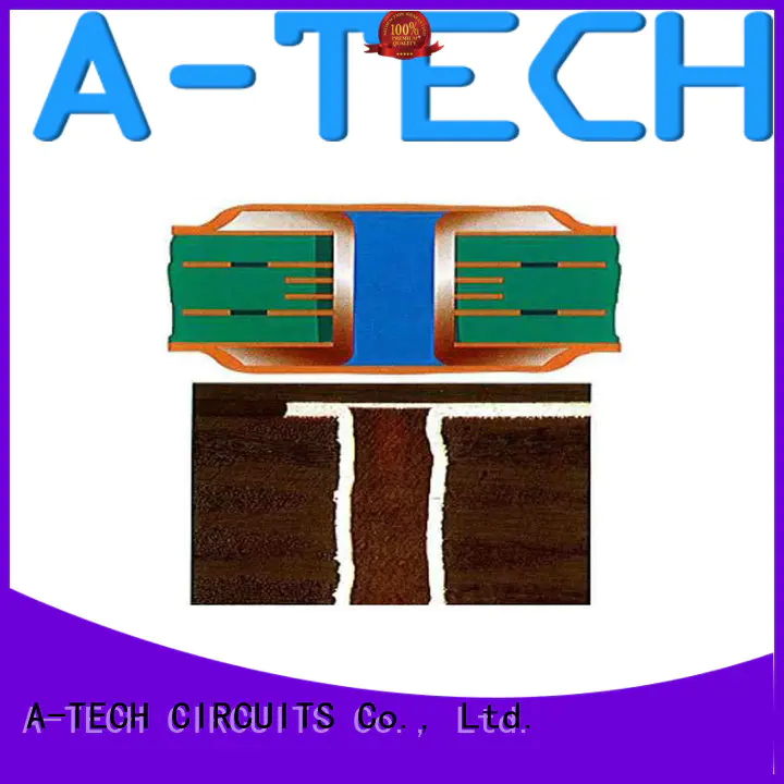
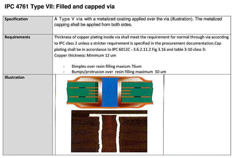
Via In Pad (VIP) technology refers to the vias in SMD pad or BGA pad due to small space for layout, in order to avoid the solder paste flow into inner layer or the other side in assembly production, basically this type of via need to be plugged with resin and plate copper over to cap the via to make it invisible.

Via in pad technology is widely used in high density PCBs, especially for the PCBs that require a limited BGA space and are focused on heat transfer and high speed design. Although blind holes and buried holes help increasing density and save space on the circuit boards, through holes are still the best choice for thermal management and high speed design elements.


The advantages of Via In Pad technology

● Suitable for fine pitch BGAs
● Improved thermal dissipation
● Provides a flat, coplanar surface for component attachment
● Leading to higher density of PCBs and promoting space saving
● Overcomes high speed design issues and constraints.
● Meets closely packed placement requirements.


The Via In Pad technology is defined in IPC standard with IPC-4761 VII


buried hybrid pcb hybrid hot-sale top supplier-1


A-TECH manufactured lots of multilayer PCBs with Via In Pad designs Both in BGA Pads or in other SMD Pads, we’re able to plugged vias fully and then plated copper over to make the surface of pad as flat as other pads without dimples.


Company Features
1. Over the years, A-TECH CIRCUITS Co., Ltd. has experienced a rapid development for its hybrid pcb by strong capability of circuit board assembly.
2. As a leader in China's impedance control pcb field, A-TECH CIRCUITS Co., Ltd. has a strong economic strength and excellent R&D team.
3. Our company has evolved a strategy of ongoing minimization. We reduce our impact on the environment by minimizing energy consumption, air emissions (particularly VOCs & CO2), etc. We are drawing upon our core capabilities and strengths, and collective environmental actions through collaboration with supplier and industry partners, and key stakeholders.
All manufacturing processes and test procedures of A-TECH hybrid pcb are strictly overseen by our professional workers according to the standards of building materials. The mosaics are produced in Hengsheng factory covering around 16000 square meters
A-TECH hybrid pcb is developed and constantly improved for its technical performance, making it perfectly suitable for innovative and future-oriented buildings. Hengsheng's glass mosaic tiles are applied widely, especially in kitchen, hotel and KTV
The whole process of A-TECH circuit board assembly is energy efficient. The primary processes are improved including the design of its structure and the computer control of production. The mosaics are consistent in color, sizing and finish
Very little waste is produced in the production process of A-TECH impedance control pcb because all the raw materials are optimally used due to computer-operated production. The mosaics are produced in Hengsheng factory covering around 16000 square meters
A-TECH circuit board assembly is created throughout a series of production processes which include raw material extraction, raw material process, and quality inspections. Over 2000 mosaic models have been developed
The product is able to meet the high quality requirements of many varieties of production. The mosaics vary in color
Product Message
Chat Online 编辑模式下无法使用
Chat Online inputting...
Please hold on and we will get back to you soon