A-TECH  >  AI - Page Sitemap  >  A-TECH free delivery via in pad pcb durable at discount
A-TECH free delivery via in pad pcb durable at discount

A-TECH free delivery via in pad pcb durable at discount

Types of Impedance
Single-ended, Differential, Coplanar
Testing of Impedance
Impedance coupons
Tolerance of Impedance
+/-10%
Min Order Quantity
No
Production Lead Time
5-18 Working Days
Supply Capacity
15000 ㎡/Month
Certifications
UL, ISO9001, TS16949
Payment Terms
T/T, Paypal, WU etc.
Shipment Terms
EXW, FOB, DDU etc.
Test Way
100% E-Test
Standard
IPC CLASS 2 / CLASS 3
Price
Get Latest Price
Get the latest price
Quantity Needed:
Pieces
E-mail:
Application Scope
Aluminum PCB has a wide range of applications.A-TECH always provides customers with reasonable and efficient one-stop solutions based on the professional attitude.
Company Advantages
1. A-TECH via in pad technology is manufactured with high-performance materials. Due to the applications where the product is used, only those materials with desirable combinations of mechanical characteristics are selected.
2. This product is not susceptible to temperature variations. The ingredients contained would stay lazy when the temperature changes.
3. This product features water repellency. The state-of-the-art coating and seam will block condensation and rain to penetrate through to the interior.
4. This product is widely used on account of its obvious advantage that saving people from work that is full of dullness and monotony.
5. The product eases the burden of feet when it comes to feet comfort and fit, and helps reduce the chances of the ankle, tendons, and ligament injuries.


Impedance is the combination of the capacitance and inductance of a circuit when operated at high frequency. Control impedance in printed circuit boards are used across a broad range of applications to help ensure high signal integrity. Basically there are usually three types of impedance in PCB designs like single-ended impedance, differential impedance and coplanar impedance.

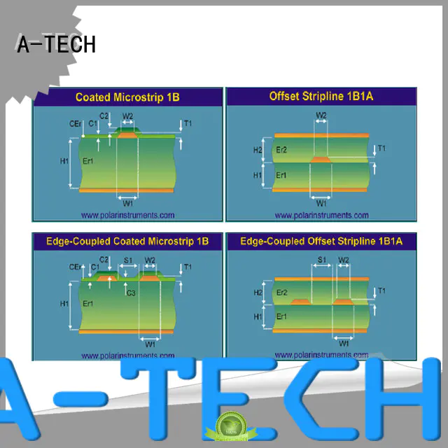
The factors affect impedance include: impedance trace width/spacing, copper thickness, dielectric thickness on either side of the impedance traces, dielectric constant of the core and prepreg material etc.

The applications of impedance control PCB include RF communication, Signal processing, High quality analog video, Computing 100MHz and above, Telecommunications and so on.

A large proportion of multilayer PCBs that A-TECH manufactured are with impedance control requirements, normally we will calculate impedance based on stack up and gerber designs to match with specified impedance values, our engineering dept might do necessary adjustments on stack up or impedance trace width/spacing if there is any mismatch after calculation. Moreover, the impedance coupons will be placed in each working panel which use for testing impedance values before shipment.


Company Features
1. A-TECH CIRCUITS Co., Ltd. is at the leading position in the industrial field.
2. The launch of via in pad pcb breaks the barriers of technology innovation.
3. A-TECH CIRCUITS Co., Ltd. deeply believes that customers are the source of long-term development for an enterprise. Inquire! Unremitting efforts will be made by A-TECH CIRCUITS Co., Ltd. to build a stronger image of A-TECH. Inquire!
A-TECH via in pad pcb is specifically designed to meet the needs of customers, featuring innovation and functionality.
A-TECH via in pad pcb is produced with the well-selected raw materials to ensure each piece in good condition.
The production of A-TECH via in pad pcb strictly complies with ISO standard manufacturing processes.
The production of A-TECH via in pad pcb is empowered with the use of advanced tools and machines.
All indicators and processes of A-TECH via in pad pcb meet the requirements of national indicators.
The product is lightweight. It is made of extremely lightweight fabric and lightweight accessories such as zippers, and inner lining.
Product Message
Chat Online 编辑模式下无法使用
Chat Online inputting...
Please hold on and we will get back to you soon