Company Advantages1. A-TECH press fit pins pcb is quality tested in our accredited laboratories. It has passed key inspection and quality control tests such as Impact Test, Water Resistance Test, Vibration Test, Sound Insulation Test, etc. The product has the performance of great stability
2. A-TECH CIRCUITS Co., Ltd. has strong innovation ability, research ability and development ability for buried via and blind via . It can reduce the electrical signal loss and provides the highest efficiency
3. The product delivers powerful brightness. Thanks to its innovative design, the new type of illuminating elements can emit stronger brightness under the same energy consumption. It is vacuum-sealed, which can greatly reduce the bulk of the overall cargo
4. The product has a smooth surface without bumps. All parts are welded seamlessly together welding materials and are grinded and polished. It has passed AOI which ensures there will be no errors or welding defects
5. The product features desirable safety. The ammonia refrigerant used has a characteristic odor that can be detected by humans even at very low concentrations. It is widely used in different electronics industries, such as telecommunication and consumer electronics
PCB with Blind and Buried Vias
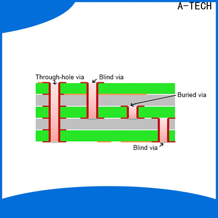
Basically the blind and buried vias are popular to be designed on high density PCBs due to the limit of small space, the blind and buried vias can only pass through necessary layers and more surface area become available for components, they have the ability to meet the density constraints of line and pads on a typical design without increasing the layer count or board size and reduce the PCB aspect ratio for convenient production.
Blind Vias
Blind via is a copper plated hole that connects only one outer layer to one or more inner layers, it never goes all the way through a circuit board but only visible on one side of circuit boards. The blind via can be laser or mechanically drilled based on the detailed via hole size and layer stackup.
Buried Vias
Buried Via is a copper plated hole that connects two or more inner layers without contacting the outer layers, as the name suggests, it’s buried inside, so it’s not visible from the outer layer of PCB. Buried via has no impact to any trace or surface mount component on the top or bottom layers, trace or SMD pad can be placed directly over the buried via.
A-TECH CIRCUITS has capacity to build both of blind via and buried via with different demands, We’ll use laser drill for the blind vias with size smaller than 150um and use mechanical drill for the blind via size larger than 150um, the technology of blind via we can achieve include via in pad, stacked via and staggered via. The minimum size of buried via normally need to be 150um and they’ll be plugged with resin to avoid prepreg flow into buried via which might affect the connection with adjacent layers.
Company Features1. A-TECH CIRCUITS Co., Ltd. is a modern enterprise specialized in buried via and blind via production. We have set up a team of experts in production. They demonstrate their strong expertise in product design, manufacturing, overall production flow, and packaging.
2. Our team of manufacturing members contributes to our business success. They utilize various processing technologies to manufacture products at the highest level and within the lead time.
3. Our company has set up a group of talented engaged employees. They are equipped with manufacturing skills and knowledge, with the right attitude to ensure that we can bring the best results for our customers. Our final goal is selling products in every corner of the world. We are making much effort in realizing it by cultivating the customer service team, improving our R&D capability, and developing more valuable marketing channels.
