Company Advantages1. The design of A-TECH castellated holes pcb is based on humanistic functionalism that is pursued in the furniture industry. It attaches great importance on user experience, including elements of materials, texture, style, practicality, and color harmoniousness.
2. The product has the unique built-in technology which is conducive to control the LED working temperature and thus maximize its service life.
3. Any defect of the product has been avoided or eliminated during our strict quality assurance procedure.
4. This product will definitely generate a higher sale. It will aid a company to develop a professional image of their merchandise and boost sales.
5. It expands the scope of customers. It helps attract a vast number of potential customers from the delivery guy to the customer, to people passing by the mailing boxes, who would otherwise not be attracted if the merchandise is delivered in plain boxes.
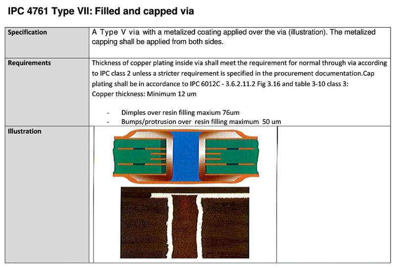
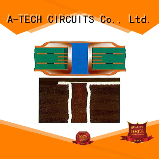
Via In Pad (VIP) technology refers to the vias in SMD pad or BGA pad due to small space for layout, in order to avoid the solder paste flow into inner layer or the other side in assembly production, basically this type of via need to be plugged with resin and plate copper over to cap the via to make it invisible.
Via in pad technology is widely used in high density PCBs, especially for the PCBs that require a limited BGA space and are focused on heat transfer and high speed design. Although blind holes and buried holes help increasing density and save space on the circuit boards, through holes are still the best choice for thermal management and high speed design elements.
The advantages of Via In Pad technology
● Suitable for fine pitch BGAs
● Improved thermal dissipation
● Provides a flat, coplanar surface for component attachment
● Leading to higher density of PCBs and promoting space saving
● Overcomes high speed design issues and constraints.
● Meets closely packed placement requirements.
The Via In Pad technology is defined in IPC standard with IPC-4761 VII

A-TECH manufactured lots of multilayer PCBs with Via In Pad designs Both in BGA Pads or in other SMD Pads, we’re able to plugged vias fully and then plated copper over to make the surface of pad as flat as other pads without dimples.
Company Features1. A-TECH PCB provides customers with a variety of
thick copper pcb .
2. A-TECH CIRCUITS Co., Ltd. has kept up with more advanced technology in manufacturing.
3. We are committed to making our living environment a more sustainable world. By making efforts in changing the production model and adopting energy-efficient facilities, we have confidence to realize our mission. Our company is committed to reducing the environmental impact of our businesses and promoting the sustainable development of natural resources. To achieve this mission, we will conduct business in accordance with applicable environmental laws, regulations, and policies. Our business philosophy is to provide our customers with the highest level of products and services. We constantly work with our clients by providing effective solutions and cost benefits. Improving customer satisfaction is our foremost mission. Through establishing close partnerships with our clients and enhancing communication, we can offer the most targeted product solutions that are suitable for them.

