Company Advantages1. A-TECH heavy copper pcb undergoes different types of evaluation and testing. This involves the evaluation and testing of its shape and design, electric shock hazard, and whether sharp edges or points can result in user injury.
2. This product is user-friendly. Factors of the user such as the dimension of the user, safety, and user feeling are concerned because the furniture is a product that directly or indirectly contacts with the user.
3. The product has the needed stretch. Its fabric shows proper elasticity without exposing elastic fibers or broken stitches during the stretch test.
4. A-TECH has built a complete quality assurance system and has got heavy copper pcb certificate of quality control system.
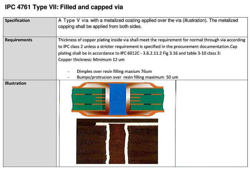
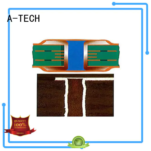
Via In Pad (VIP) technology refers to the vias in SMD pad or BGA pad due to small space for layout, in order to avoid the solder paste flow into inner layer or the other side in assembly production, basically this type of via need to be plugged with resin and plate copper over to cap the via to make it invisible.
Via in pad technology is widely used in high density PCBs, especially for the PCBs that require a limited BGA space and are focused on heat transfer and high speed design. Although blind holes and buried holes help increasing density and save space on the circuit boards, through holes are still the best choice for thermal management and high speed design elements.
The advantages of Via In Pad technology
● Suitable for fine pitch BGAs
● Improved thermal dissipation
● Provides a flat, coplanar surface for component attachment
● Leading to higher density of PCBs and promoting space saving
● Overcomes high speed design issues and constraints.
● Meets closely packed placement requirements.
The Via In Pad technology is defined in IPC standard with IPC-4761 VII

A-TECH manufactured lots of multilayer PCBs with Via In Pad designs Both in BGA Pads or in other SMD Pads, we’re able to plugged vias fully and then plated copper over to make the surface of pad as flat as other pads without dimples.
Company Features1. A-TECH CIRCUITS Co., Ltd. has been widely known in the
impedance control pcb marketplace.
2. Our company has received a number of prestigious awards voted by clients. In an age when manufacturing service is more and more demanding, it’s fantastic to be appreciated and supported by our clients.
3. We will work together to create sustainable value with everything we do – together with our employees, partners, and stakeholders. To embrace green production, we have adopted different plans. We will encourage reuse, recycle, and recovery of resources during production, which helps us decrease the amount of waste that ends up in the landfill. Our sustainability strategy has been shared across departments. All our members are focusing on improving the way we manufacture and design our products to help reduce our impact on the environment. We promote our sustainable development in our business. We make sure that our use of energy, raw material, and natural resources are legal and environmentally friendly.

