Latest products
Where is the importance of the PCB circuit board plugging process?
by:A-TECH
2021-03-10
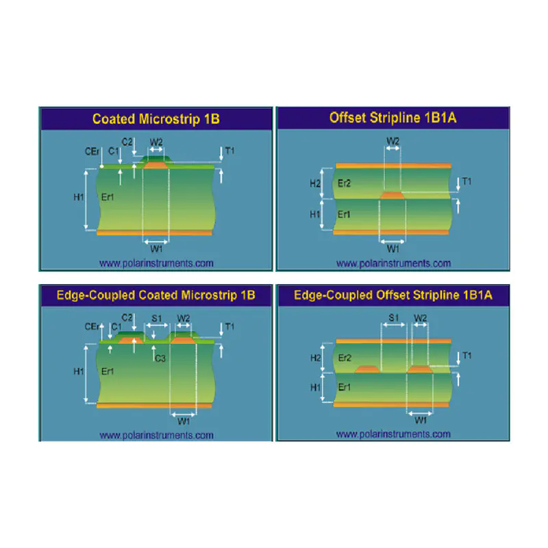
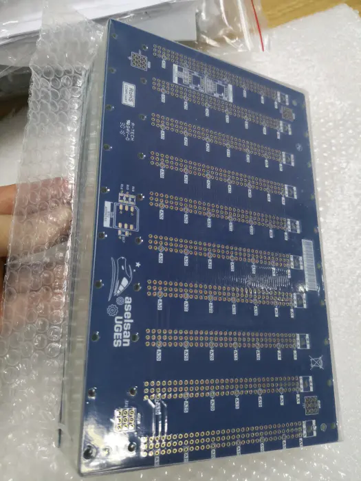
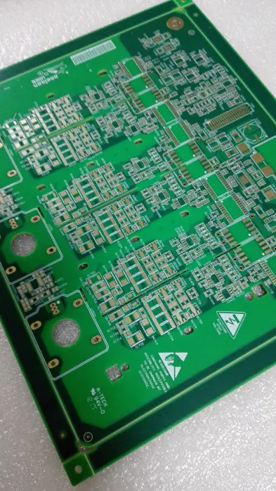
With the development of electronic products in the direction of 'light, thin, short, and smallThe process is long and process control is difficult. So, where is the importance of the PCB circuit board plugging process? 1. The hole plugging process should meet the following requirements: 1. There is copper in the via hole, and the solder mask can be plugged or not plugged. 2. There must be tin and lead in the via hole, with a certain thickness requirement (4 microns), and no solder mask ink should enter the hole, causing tin beads to be hidden in the hole. 3. The through hole must have solder mask ink plug hole, opaque, no tin bead, flatness and other requirements. 4. For surface mount boards, especially BGA and IC mounting, the via hole plug holes must be flat, convex and concave plus or minus 1 mil, and there must be no red tin on the edge of the via hole, and tin beads in the via hole, etc. phenomenon. 2. The plugging process mainly has the following functions: 1. Preventing the short circuit caused by the tin passing through the component surface through the through hole when the PCB is over wave soldering; if the via is placed on the BGA pad, the plugging must be made first, and then gold-plated Handling to facilitate the welding of BGA. 2. Avoid flux residue in the vias. 3. Prevent the surface solder paste from flowing into the hole to cause false soldering, which will affect the placement. 4. Prevent the tin bead from popping up during wave soldering, causing short circuit. Through the above analysis of the requirements and functions of the plugging process, the importance of the PCB circuit board plugging process is reflected. Have you mastered it?
Custom message