Latest products
What Is Osp
by:A-TECH
2020-09-02
Depending on the capabilities of the board factory and the standard of the board, some boards that exceed the shelf life can be returned to the board. The factory washes off the old OSP on the PCB floor and then re-provides a new OSP. However, washing out the old OSP requires more corrosive chemical compounds, which is able to injury the copper floor kind of. Therefore, if the solder pad is just too small to be processed, it should talk with the board producer whether it may be resurfaced.
The current invention pertains to the meeting of PCBs and to the therapy of OSP coatings used during the manufacturing of PCBA. In particular, the present invention offers improved methods of eradicating OSP coatings prior to reflow soldering that overcome the disadvantages famous above with respect to the prior artwork. The improved methodology of the present invention includes utilizing a plasma environment to deal with and remove the OSP coating. There are two main strategies used to take away the OSP layer before reflow soldering, both of which have disadvantages. In a primary technique, a special chemical solvent may be utilized to the OSP layer previous to solder paste printing.
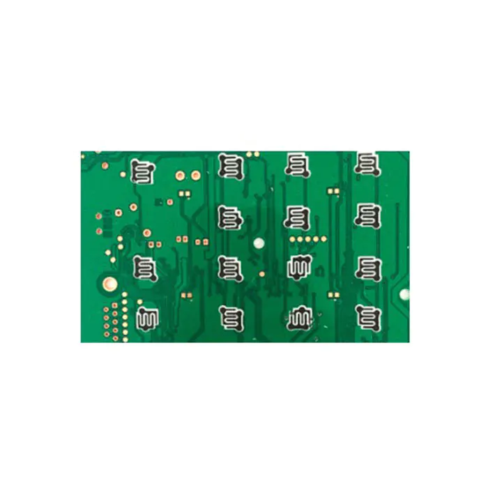
Be certain to have your board refinished with a sizzling-solder dip, purchase components that aren't pure tin plated, and consider selecting a different finish like Lead Free HASL, OSP, or ENIG. Generally talking, after the completion of the OSP, the shelf life of the OSP is up to six months, and a few are only three months.
This solvent acts to dissolve the OSP layer and put together the copper pad floor for solder paste printing. Disadvantages of this method embody an additional operation step that adds to the time, materials and vitality costs related to manufacturing. As famous the conductive layers for a PCB are generally created from a thin copper foil layer that has been patterned to create the traces used to connect and interconnect the digital elements. Originally, elements included leads that were mounted and soldered into holes drilled into the PCB to contact the conducting copper layer.
This drilling course of requires very exact, very small mechanical bits, or very accurate laser drilling methods. There is a low however measurable incidence of gold-to-nickel adhesion failure. This known as “black nickel” or “black pads” because, not surprisingly, the floor of the nickel turns black. The immersion gold on the pad floor seems normal and solder wets to the gold quite easily.
Custom message