What details should be paid attention to when calculating impedance in PCB design?
by:A-TECH
2021-04-07
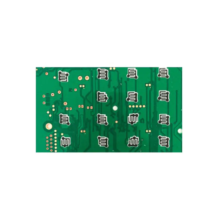
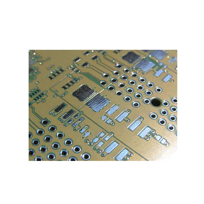
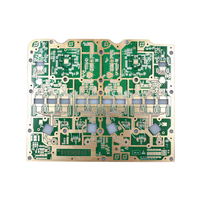
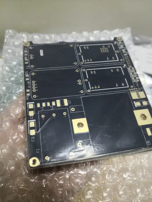
In PCB design, impedance is an inevitable problem. So, what details should be paid attention to when calculating impedance in PCB design? 1. The line width is rather wide than thin. Because there is a fine limit in the process, there is no limit to the width. In the later stage, in order to adjust the impedance, it will be troublesome to adjust the line width and reach the limit, which will increase the cost or relax the impedance control. 2. There is a trend overall. There may be multiple impedance control targets in the design, so the overall size is too large or too small, and there is no need to be too large or small out of sync. 3. Consider the residual copper rate and the amount of glue flow. When one or both sides of the prepreg are etched circuits, the glue will fill the etched gaps during the pressing process, so that the glue thickness time between the two layers will be reduced. The residual copper rate and the amount of glue flow are not calculated correctly, and the dielectric coefficient of the new material is inconsistent with the nominal value, which may cause signal integrity problems. 4. Specify the glass cloth and glue content. The dielectric coefficient of different glass cloths, prepregs or core boards with different glue content is different, even if it is about the same height, there may be a difference between 3.5 and 4. This difference can cause a single-line impedance change of about 3 ohm. The above are the details that need to be paid attention to in PCB design and calculation of impedance. I hope to help everyone.
Custom message