What are the methods of PCB vias?
by:A-TECH
2021-03-15
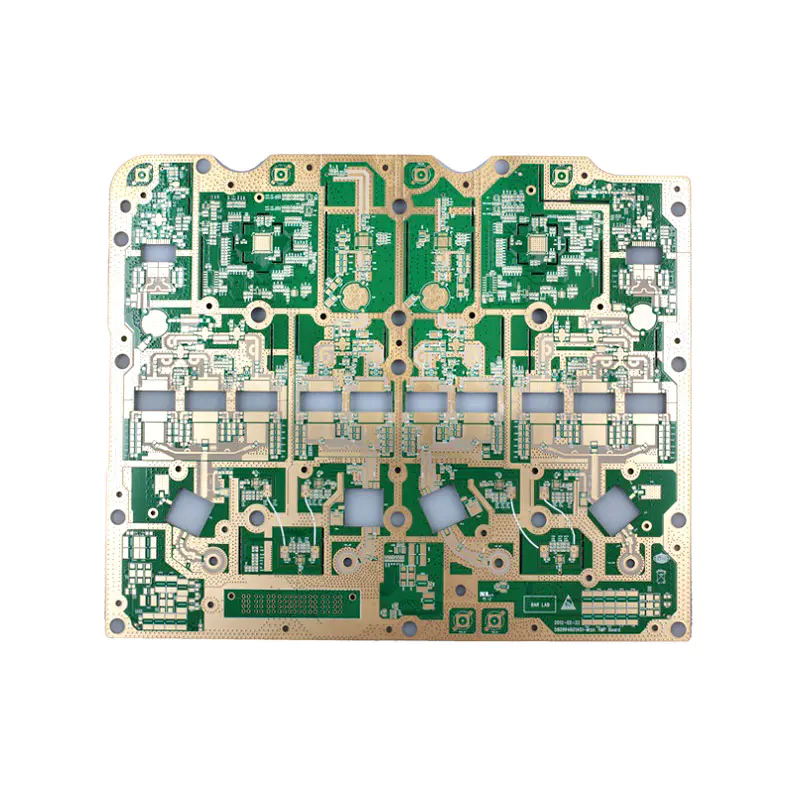
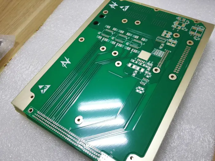
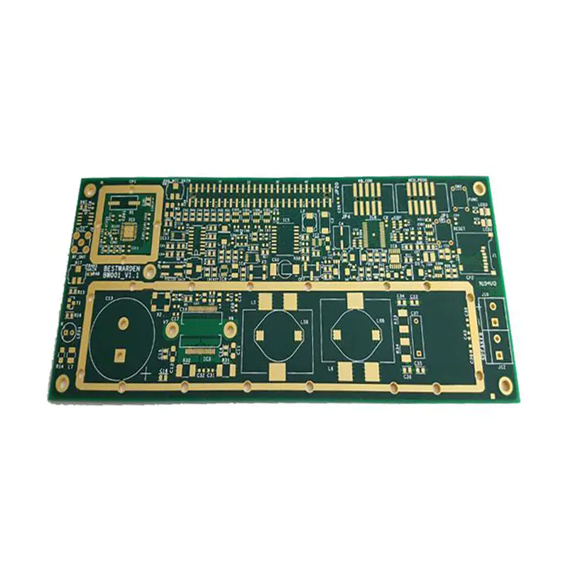
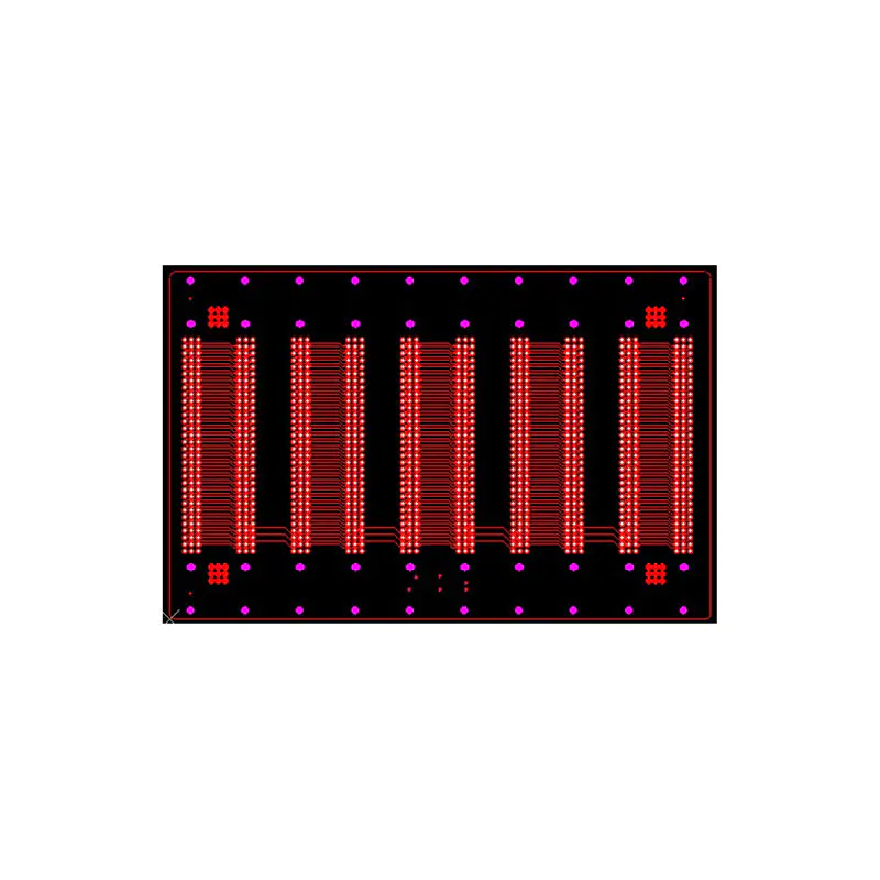
Speaking of PCB, I believe everyone will feel that it can be seen everywhere in our lives, from almost all household appliances, various accessories in computers, to various digital products, as long as it is electronic products almost all use PCB. Circuit boards are classified into single-layer boards and multi-layer boards. Each layer is made up of layers of copper foil circuits. If this is the case, how are the layers connected? Here is an extension of the industry term called vias, which means that the manufacture of circuit boards uses drilling to connect to different circuit layers. The purpose of connection is to conduct electricity, so it is called vias for PCB proofing. To conduct electricity, a layer of conductive material must be electroplated on the surface of the drilled hole. The commonly used electrical material is copper. Through this manufacturing process, electrons can move between different copper foil layers. So, what are the ways of PCB vias? The first is the through hole of the circuit board. The through hole of PCB proofing is also a commonly used one. By directing the pcb to the light, the hole that can see the bright light is the through hole. This is also a relatively simple hole for PCB proofing. During the production process, a drill or laser is used to directly drill the circuit board. The required cost is also relatively cheap. However, although the through hole is cheap, it often uses more PCB space. The second is the blind hole of PCB proofing, that is, the outermost circuit of the PCB and the adjacent inner layer are connected by plating holes. Because the opposite side cannot be seen, the blind hole called PCB proofing is also a commonly used one. In order to increase the space utilization of the pcb circuit layer, there is also a blind via process. It should be noted that the PCB proofing method requires special attention to the depth of the drilling to be just right. You can drill holes in the circuit layers that need to be connected in the individual circuit layers in advance, and then glue them together, but it needs to be compared. Precise positioning and alignment device. The third is PCB buried vias, which connect any circuit layer inside the PCB but not conduct to the outer layer. This process cannot be achieved by drilling after bonding. It must be drilled at the time of individual circuit layers. After the inner layer is partially bonded, it must be electroplated before it can be fully bonded. Compared with the above through holes and blinds The hole method is more labor intensive, so its price is also expensive. Because this process is usually only used in high-density circuit boards to increase the usable space of other circuit layers. With the development of electronic products in the direction of 'light, thin, short, and smallThe circuit board via hole must be plugged? In order to respond to customer requirements in a timely manner, after a lot of practice, the traditional aluminum plugging process was changed, and the circuit board surface solder mask and plugging were completed with white mesh, so that the production is more stable and the quality is more guaranteed. PCB has always insisted on using superb technical force, sophisticated production equipment, perfect testing methods, product quality higher than industry standards, and warm and thoughtful service, which has won praise and welcome from global merchants and users.
Custom message