What are the manufacturing processes for double-sided PCB circuit boards?
by:A-TECH
2021-03-26
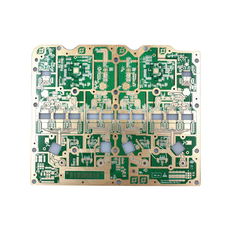
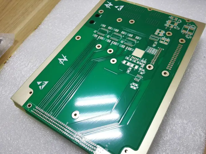
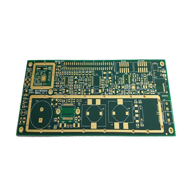
The double-sided board is a PCB circuit board that is used more frequently, and its manufacturing process is more complicated. So, what are the manufacturing processes for double-sided PCB circuit boards? 1. Graphic electroplating process: Foil clad board --> blanking --> punching and drilling benchmark holes --> CNC drilling --> inspection --> deburring --> electroless thin copper plating --> electroplating thin copper- -> Inspection --> Brushing --> Filming (or screen printing) --> Exposure and development (or curing) --> Inspection and repairing --> Graphic plating --> Film removal --> Etching --> Inspection Repair board-->Plug nickel plating and gold plating-->Hot melt cleaning-->Electrical continuity detection-->Cleaning treatment-->Screen printing solder mask pattern-->Curing-->Screen printing marking symbol-->Curing --> Shape processing --> Washing and drying --> Inspection --> Packaging --> Finished product. Note: The two processes of 'electroless plating of thin copper --> electroplating of thin copper' can be replaced by the 'electroless plating of thick copper' process, both have their own advantages and disadvantages. 2 SMOBC process: The main advantage of the bare copper-clad solder mask process (SMOBC) is to solve the short-circuit phenomenon of solder bridging between thin lines. At the same time, due to the constant ratio of lead to tin, it has better solderability and storage than hot melt plates. Sex. The basis of the SMOBC process is to first produce a bare copper hole metallized double panel, and then apply hot air to level it. There are many methods for manufacturing SMOBC boards. The following mainly introduces the pattern plating method and then the lead and tin process and the hole plugging process: (1) The pattern plating method and the lead and tin process are similar to the pattern plating process, and only change after etching: double Surface copper clad board --> According to the pattern electroplating process to the etching process --> Lead and tin removal --> Inspection --> Cleaning --> Solder mask pattern --> Nickel-plated plug and gold-plated plug --> Plug tape- -> Hot air leveling --> Cleaning --> Screen printing marking symbols --> Shape processing --> Washing and drying --> Finished product inspection --> Packaging --> Finished product. (2) Hole plugging process: double-sided foil-clad board --> drilling --> electroless copper plating --> whole board copper electroplating --> plugging holes --> screen printing imaging (positive image) --> etching --> To remove the screen printing material, remove the hole blocking material --> Cleaning --> Solder mask pattern --> Nickel-plated, gold-plated plug --> Tape on the plug --> Hot air leveling --> The following procedures are the same as above To the finished product. Note: The process steps of this process are relatively simple, and the key is to plug the holes and clean the ink that plugs the holes. The above is the double-sided PCB circuit board manufacturing process detailed by professional PCB engineers. Have you mastered it?
Custom message