
The function of each layer in PCB design
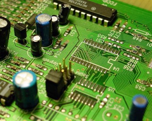
⑴Signal layer: mainly used to place components or wiring. Protel DXP usually contains 30 middle layers, namely Mid Layer1 ~ Mid Layer30, the middle layer is used to lay out the signal lines, and the top and bottom layers are used to place components or copper.
⑵Protection layer: It is mainly used to ensure that no tin plating is required on the circuit board, so as to ensure the reliability of the circuit board operation. Among them, Top Paste and Bottom Paste are the top solder mask and bottom solder mask respectively; Top Solder and Bottom Solder are solder paste protective layer and bottom solder paste protective layer respectively.
⑶Silk screen layer: mainly used to print the serial number, production number, company name, etc. of components on the printed circuit board.
⑷Inner layer: mainly used as a signal wiring layer, Protel DXP contains a total of 16 internal layers.
⑸Other layers: mainly including 4 types of layers.
Drill Guide (drilling orientation layer): mainly used for the position of drilling holes on the printed circuit board.
Keep-Out Layer (wiring-free layer): mainly used to draw the electrical border of the circuit board.
Drill Drawing (drilling drawing layer): mainly used to set the drilling shape.
Multi-Layer (multi-layer): mainly used to set multi-layer PCB.
General inquiries & Customer Service
Tel: 86-755-2335 9039 | Fax: 86-755-3318 0939
E-Mail: Enquiry@atechcircuit.com
Skype: atechcircuits

Headquarters: 602, Building B3, Zhimei Huizhi Industrial Park, Fuyong Street, Bao'an District, Shenzhen City, China
Copyright © 2025 A-TECH CIRCUITS Co., Ltd. | All Rights Reserved
Hello, please leave your name and email here before chat online so that we won't miss your message and contact you smoothly.


