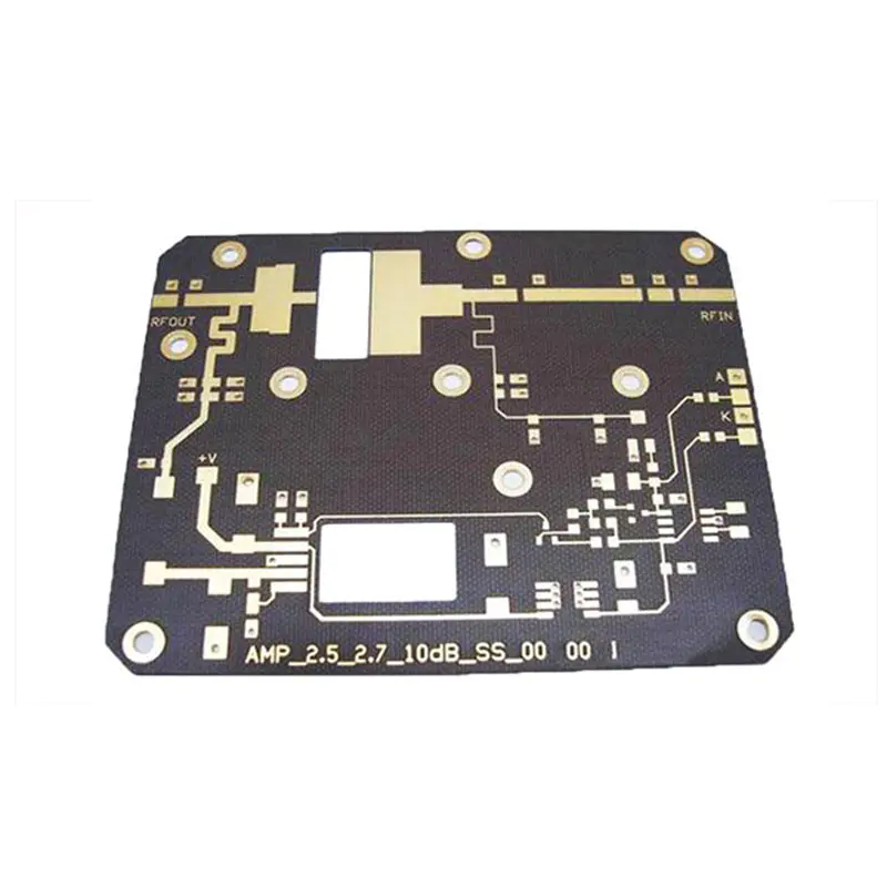
Latest products
success story of pcb assembly trend -
by:A-TECH
2020-03-03
PCB has become a fundamental element of any type of manufacturing process adopted by all leading industries around the world.As trends change and disappear, the challenge for PCB manufacturers to deliver highly customized end-to-end electronic solutions to their customer base is growing.With the advent of the year 00 s, the novelty of printed circuit boards began to build a profound concept of electrical paths on the isolation surface of the board.
The initial trend for printed circuit boards is to develop and upgrade Radio and grammar.Gradually, the concept of \"piercing technology\" appears in the picture to produce a two-sided PCB.In 1990s, PCB manufacturers in the United States introduced the idea of automotive assembly process.
This is a modern point to improve the manufacturing process with automated welding technology.R & D has accelerated the pace of end-to-end electronic solutions for defense and the US military.Most major inventions related to printed circuit boards are the core concentration of the us pcb Market.
The step of gradual upgrading in PCB manufacturing marks the great development of the electronic world.From high-speed digital and analog design to high-layer boards to high-pin-count BGA with different manufacturing methods, such as electronic mechanical components, wiring harness components, box manufacturing assembly and back panel assembly processes note the need for custom PCB in all leading industries.With cutting-edge competition, PCB manufacturers are chasing new inventions in the market and distinguishing them from the whole market, which is a huge challenge.
This may be the highlight of one of CiP (plastic circuit) inventions this is a new technology that provides an electronic manufacturing solution with an eco-friendly approach, ultra-thin and smooth PCB manufacturing process in PCB.At present, the advanced method commonly used by PCB manufacturers isof-the-art-Technology using \"surface mounting technology\", \"Integrated Circuits\" and \"hybrid circuits\" components.With the dynamic method of PCB manufacturing, various types of PCB are designed according to customer\'s requirements.
The flexibility of the manufacturing technology lies in the PCB profile, micro-drilling, material thickness, surface polishing and solder resistance capabilities.With the birth of nanotechnology, from the giant version to the micro-size, people\'s demand for things is increasing.For ten years, \"state-of-the-art technology\" has been highly applied to manufacture different types of PCB nanospheres consisting of high-performance materials, RF applications, HDI (high-density interconnect) technology, LCD (LCD) and LED (light-LEDs) technology.
With this assumption, a new custom method has been noted to provide a rare PCB manufacturing service to customers.In the printing circuit mechanization of multi-layer circuit boards, the functional design and layout have revised marks for high-end customization.The customized concept applies to PCB requirements in aircraft, defense, telecom, pharmaceutical, robotics and other industries that require flexible electronic solutions.
The main PCB assembly methods used by manufacturers are box-shaped assemblies, wire harness assemblies, and rigid/flexible PCB assemblies.Many industries now require complete turnkey solutions from material sourcing, design, prototyping to shipping orders.This enables pcb manufacturers to provide flexi solutions to customers on complete turnkey solutions and commissioned pcb assembly.
The current trend is to adopt cost-effective methods in the manufacturing process to meet the exact needs of customers.Therefore, the applicability and use of printed circuit boards used to provide electronic design and manufacturing solutions has become the main basis for minor advances and advancesThe main level of innovation
Custom message