Specification for the application of via design in high-speed PCB boards
by:A-TECH
2021-03-17
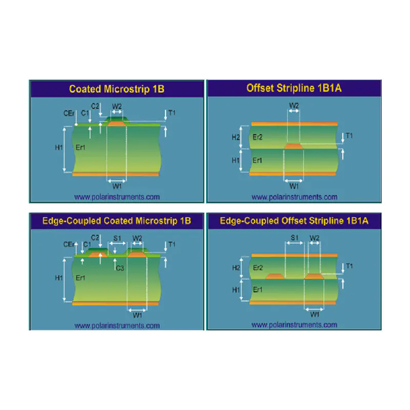
We know that in high-speed PCB design, seemingly simple vias often bring great negative effects to circuit design. Therefore, in the design, we should try our best to do the following: 1. From the two aspects of cost and signal quality, choose a reasonable size of the via. For example, for the 6-10 layer memory module PCB design, it is better to use 10/20Mil (drilled/pad) vias. For some high-density small-size boards, you can also try to use 8/18Mil. hole. Under current technical conditions, it is difficult to use smaller vias. For power or ground vias, you can consider using a larger size to reduce impedance. 2. The use of a thinner PCB is conducive to reducing the two parasitic parameters of the via. 3. Try not to change the layers of the signal traces on the PCB board, that is to say, try not to use unnecessary vias. 4. The power and ground pins should be drilled nearby, and the lead between the via and the pin should be as short as possible, because they will increase the inductance. At the same time, the power and ground leads should be as thick as possible to reduce impedance. 5. Place some grounded vias near the vias of the signal layer, so that the signal can provide the nearest loop. In addition, remember that the process needs to be flexible and changeable. The via model is a situation where there are pads on each layer. Of course, we can also reduce or even remove the pads of some layers. Especially when the density of vias is very high, it may lead to the formation of a broken groove that separates the loop in the copper layer. At this time, we can not only move the position of the via hole, but also consider reducing the soldering of the via hole on the copper layer. Disk size.
Custom message