Osp Pcb & Osp Coating Pcb
by:A-TECH
2020-09-10
The etch-back removes resin and the glass fibers so that the copper layers lengthen into the hole and as the gap is plated become integral with the deposited copper. At the glass transition temperature the resin in the composite softens and significantly increases thermal expansion; exceeding Tg then exerts mechanical overload on the board elements - e.g. the joints and the vias. Below Tg the thermal growth of the resin roughly matches copper and glass, above it gets significantly greater. As the reinforcement and copper confine the board alongside the airplane, just about all quantity enlargement tasks to the thickness and stresses the plated-through holes. Repeated soldering or other exposition to greater temperatures can cause failure of the plating, especially with thicker boards; thick boards due to this fact require a matrix with a excessive Tg.
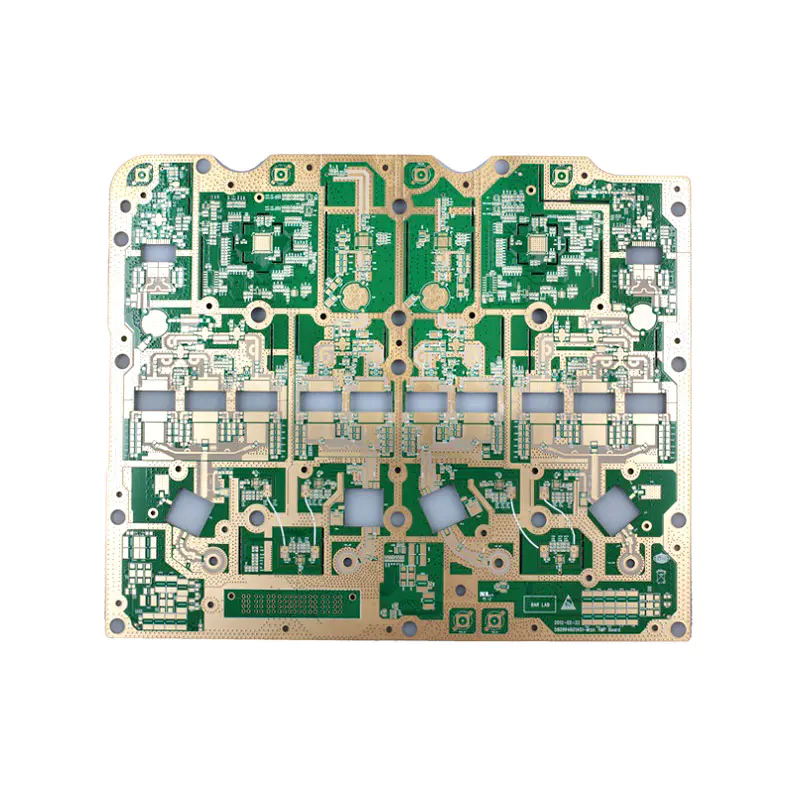
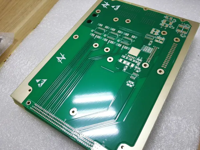
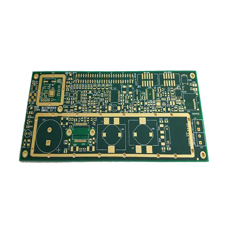
Surface mounting is used for transistors, diodes, IC chips, resistors and capacitors. Through-gap mounting could also be used for some massive elements such as electrolytic capacitors and connectors. PCBs can be single-sided (one copper layer), double-sided (two copper layers on each side of 1 substrate layer), or multi-layer (outer and internal layers of copper, alternating with layers of substrate). Multi-layer PCBs enable for a lot greater element density, because circuit traces on the inner layers would in any other case take up surface space between elements.
The rise in reputation of multilayer PCBs with more than two, and particularly with greater than 4, copper planes was concurrent with the adoption of floor mount know-how. However, multilayer PCBs make repair, evaluation, and area modification of circuits rather more troublesome and normally impractical. High-frequency PCBs refer to a general PCB design element, rather than a sort of PCB development just like the previous models. High-frequency PCBs are circuit boards which might be designed to transmit indicators over one gigahertz. As we discussed above the printed circuit boards are digital circuit boards for mounting digital parts on a non-conductive board, and for creating conductive connections between them.
When a PCB has no parts put in, it's much less ambiguously referred to as a printed wiring board (PWB) or etched wiring board. A PCB populated with electronic elements is called a printed circuit meeting (PCA), printed circuit board meeting or PCB assembly (PCBA). In informal usage, the time period 'printed circuit board' mostly means 'printed circuit meeting' (with components). The IPC most well-liked time period for assembled boards is circuit card assembly (CCA), and for assembled backplanes it's backplane assemblies. 'Card' is one other broadly used informal time period for a 'printed circuit assembly'.
'Through hole' parts are mounted by their wire leads passing by way of the board and soldered to traces on the opposite aspect. 'Surface mount' parts are attached by their results in copper traces on the identical facet of the board.
Custom message